


AT89S52 Microcontroller:Applications, Features and Datasheet
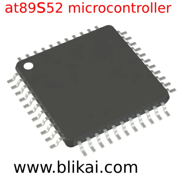
at89s52 Microcontroller
Product Overview
Blikai Part Number:AT89S52-24AI
Manufacturer: Microchip Technology
Description: IIC MCU 8BIT 8KB FLASH 44TQFP
Detailed Description :8051 89S Microcontroller IC 8-Bit 24MHz 8KB (8K x 8) FLASH 44-TQFP (10x10)
Lead Time: Can Ship Immediately
Category: Microcontrollers
Short Description
The gadget is crafted utilizing Atmel’s high-density nonvolatile memory tech and aligns with the standard 80C51 instruction set and pinout widely used in the industry. The embedded Flash enables reprogramming of the program memory either in-system or through a conventional nonvolatile memory programmer. Through integrating a versatile 8-bit CPU with in-system programmable Flash on a single chip, the Atmel AT89S52 emerges as a potent microcontroller, offering a remarkably adaptable and economical solution for numerous embedded control tasks.
The AT89S52 comes equipped with the following standard features: 8K bytes of Flash memory, 256 bytes of RAM, 32 I/O lines, a Watchdog timer, two data pointers, three 16-bit timer/counters, a six-vector two-level interrupt structure, a full duplex serial port, an on-chip oscillator, and clock circuitry. Additionally, the AT89S52 incorporates static logic enabling operation down to zero frequency and supports two software-selectable power-saving modes. The Idle Mode halts the CPU while permitting the continued operation of the RAM, timer/counters, serial port, and interrupt system. The Power-down mode preserves the contents of the RAM while halting the oscillator, deactivating all other chip functionalities until the occurrence of the next interrupt or hardware reset.
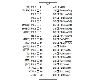
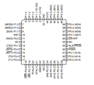
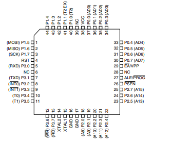
AT89S52 Pin Configurations
40-lead PDIP
44-lead PLCC
44-lead TQFP
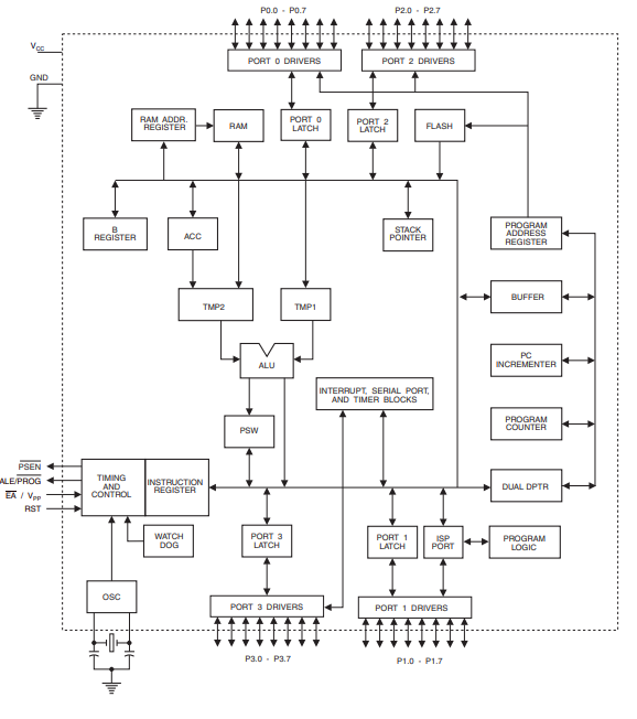
Block Diagram
Product Specifications
All trademarks, brands, and logos mentioned on this platform are utilized with the consent of their rightful owners. Their inclusion does not suggest any form of association or endorsement with any of the brands, trademarks, or logos portrayed, described, or associated with products showcased here.
| Manufacturer | Microchip Technology |
| Category | Integrated Circuits (ICs) - Embedded - Microcontrollers |
| Fully Static Operation | 0 Hz to 33 MHz |
| Operating Range | 4.0V to 5.5V |
| level | Three-level Program Memory Lock |
| RAM | 256 x 8-bit Internal RAM |
| MCS®-51 Products | Compatible |
| In-System Programmable (ISP) Flash Memory | 8K Bytes |
| – Endurance | 10,000 Write/Erase Cycles |
| Programmable I/O Lines | 32 |
| Timer/Counters | Three 16-bit |
| Interrupt Sources | Eight |
| UART Serial Channel | Full Duplex |
| / | Low-power Idle and Power-down Modes |
| Interrupt Recovery from Power-down Mode | / |
| / | Watchdog Timer |
| / | Dual Data Pointer |
| / | Power-off Flag |
| / | Fast Programming Time |
| / | Flexible ISP Programming (Byte and Page Mode) |
| Packaging Option |
Green (Pb/Halide-free) |
AT89S52 Pin Specification
Memory Arrangement
MCS-51 microcontroller units feature distinct address spaces for Program and Data Memory, allowing for addressing of up to 64K bytes each of external Program and Data Memory.
Program Memory
When the EA pin is grounded, all program fetches are routed to external memory. On the AT89S52, if EA is linked to VCC, program fetches to addresses 0000H through 1FFFH are directed internally, while fetches to addresses 2000H through FFFFH are directed externally.
Data Memory
The AT89S52 integrates 256 bytes of on-chip RAM. The upper 128 bytes share a parallel address space with the Special Function Registers (SFRs). Thus, the upper 128 bytes share the same addresses as the SFR space but are physically distinct from it.
When an instruction accesses an internal location beyond address 7FH, the address mode specified in the instruction determines whether the CPU accesses the upper 128 bytes of RAM or the SFR space. Instructions utilizing direct addressing access the SFR space. For instance, the direct addressing instruction below accesses the SFR at location 0A0H (P2).
MOV 0A0H
Instructions employing indirect addressing access the upper 128 bytes of RAM. For example, the following indirect addressing instruction, where R0 holds 0A0H, accesses the data byte at address 0A0H instead of P2.
MOV @R0
It's worth noting that stack operations exemplify indirect addressing, hence the upper 128 bytes of data RAM serve as stack space.
AT89S52 Applications
●Sensor Systems
●Medical systems
●Home automation systems
●Low-cost embedded systems
●Automobiles
●Defense and safety purposes
●Multiple DIY Projects
●Very good choice if you are learning ATmel
●Projects requiring Multiple I/O interfaces and communications
●Replacement for Arduino Module
●Ideal for more advanced level A/D applications in automotive, industrial, appliances, and consumer applications.
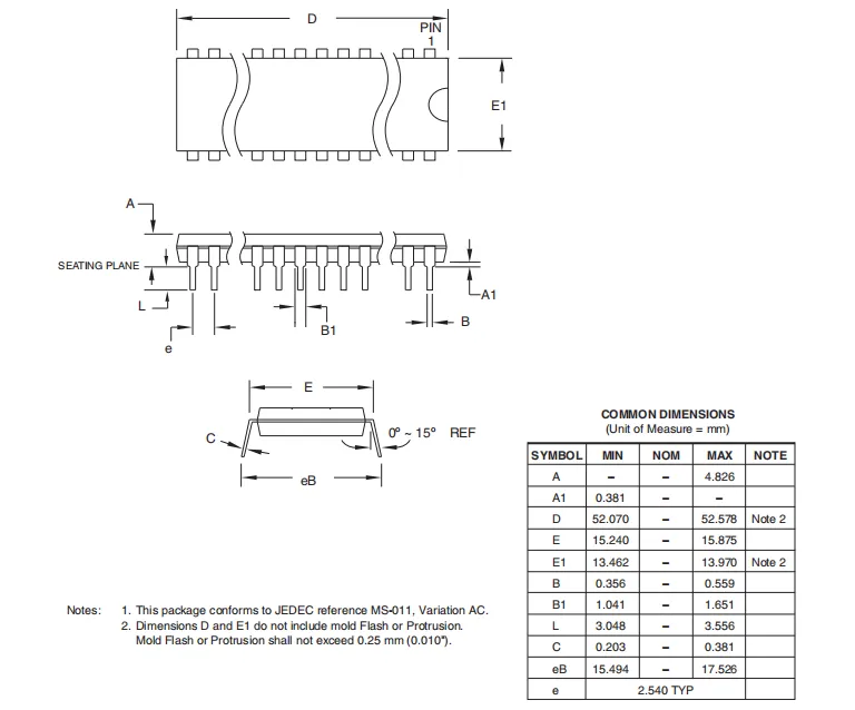
AT89S52 Package
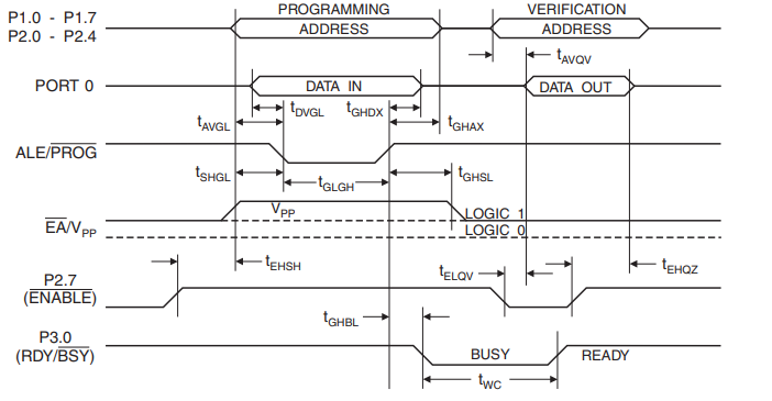
Flash Programming and Verification Waveforms – Parallel Mode
Manufacturer of AT89S52
Microchip Technology Inc. is a publicly traded American corporation renowned for manufacturing microcontrollers, mixed-signal, analog, and Flash-IP integrated circuits.
The extensive range of Microchip's products encompasses microcontrollers such as PIC, dsPIC, AVR, and SAM series, alongside serial EEPROM and SRAM devices, embedded security solutions, radio frequency (RF) devices, analog components for thermal, power, and battery management, as well as linear and interface and wireless products.
Headquartered in Chandler, Arizona, Microchip operates fabrication facilities (fabs) in Tempe, Arizona, Gresham, Oregon, and Colorado Springs, Colorado. Additionally, its assembly and testing facilities are situated in Chachoengsao, Thailand, as well as Calamba and Cabuyao in the Philippines.
Oscillator Characteristics
XTAL1 and XTAL2 serve as the input and output, respectively, of an inverting amplifier configurable for use as an on-chip oscillator, depicted in Figure 16-1. Either a quartz crystal or ceramic resonator is suitable for this purpose. When driven by an external clock source, XTAL2 should remain unconnected while XTAL1 is driven, as illustrated in Figure 16-2. The duty cycle of the external clock signal is immaterial since the input to the internal clocking circuitry employs a divide-by-two flip-flop. However, adherence to minimum and maximum voltage high and low time specifications is essential.
Idle Mode
During idle mode, the CPU enters a sleep state while all on-chip peripherals remain operational. Activation of this mode is initiated by software. The contents of the on-chip RAM and special function registers remain unaltered throughout idle mode. Termination of idle mode can occur via any enabled interrupt or a hardware reset. It's noteworthy that upon termination by a hardware reset, the device typically resumes program execution from up to two machine cycles before the internal reset algorithm assumes control. While on-chip hardware blocks access to internal RAM during this event, access to the port pins remains unrestricted. To prevent inadvertent writes to a port pin or external memory upon termination of idle mode by a reset, the instruction succeeding the one that triggers idle mode should refrain from writing to a port pin or external memory.
Power-down Mode
In power-down mode, the oscillator ceases operation, with the instruction invoking power-down being the last one executed. The on-chip RAM and special function registers maintain their values until power-down mode is terminated. Exiting power-down mode can be initiated either by a hardware reset or an enabled external interrupt. A reset redefines the special function registers but does not alter the on-chip RAM. Activation of the reset should only occur after VCC returns to its normal operating level and should be sustained long enough to enable the oscillator to restart and stabilize.
Final Thoughts
Blikai.com offers top-quality AT89S52-24AI components manufactured by Microchip Technology. To ensure reliability and performance, our parts are subjected to stringent quality control. There is an active state for the AT89S52-24AI Microcontrollers. Surface Mount is the preferred installation method for the AT89S52-24AI.
The AT89S52-24AI Inventory quantity, preferential price, datasheet, and manufacturer can all be obtained by email if you still need to find what you were looking for. You can always reach out to us if you have any questions.


