


IC7400:Description,Features,Application and FAQ
The IC7400 holds the distinction of being the most widely embraced logic family within integrated circuits. Texas Instruments initiated this product line with the launch of the SN5400 series TTL (transistor-transistor logic) chip in 1964. Subsequently, in 1966, the SN7400 series logic chip followed suit. These chips swiftly captured over 50% of the logic chip market. Over time, they evolved into steadfast electronic components. In the ensuing decade, various pin-compatible iterations and descendant families emerged, catering to lower-power supply voltages, low-power CMOS technology, and surface-mount packages. This article offers an introduction to the IC 7400.
What is IC 7400?
IC 7400 encompasses a range of devices, offering a spectrum of functionalities from fundamental logic gates and flip-flops to counters, ALUs, and bus transceivers. Part of the extensive digital IC family known as the 7400 series, these ICs comprise various discrete logic components such as logic gates, registers, RAM units, and decoders.
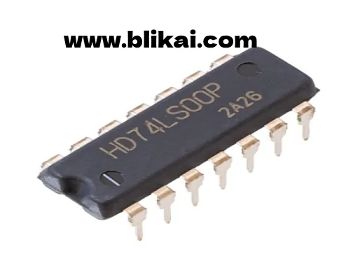
With 14 pins, IC 7400 comprises four 2-input NAND gates. Each gate employs 2 input pins and 1 output pin, with the remaining 2 pins designated for power and ground connections. This chip is available in diverse packages including surface mount and through-hole options, such as ceramic or plastic dual-in-line and flat pack configurations.
IC 7400 Pin Configuration
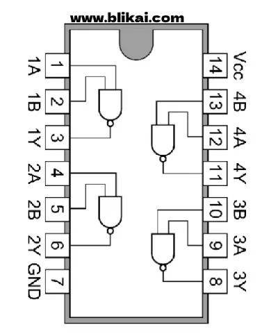
The pin configuration of the 7400 IC is outlined as follows:
- Pin 1: A-input for Gate 1
- Pin 2: B-input for Gate 1
- Pin 3: Y-output for Gate 1
- Pin 4: A-input for Gate 2
- Pin 5: B-input for Gate 2
- Pin 6: Y-output for Gate 2
- Pin 7: Ground terminal (GND)
- Pin 8: Y-output for Gate 3
- Pin 9: B-input for Gate 3
- Pin 10: A-input for Gate 3
- Pin 11: Y-output for Gate 4
- Pin 12: B-input for Gate 4
- Pin 13: A-input for Gate 4
- Pin 14: Vcc pin (Positive Supply)
Recommended Operating Conditions
Electrical Characteristics
Switching Characteristics at Vcc=5V,Ta=25°C
Pin Description
IC 7400 Specifications
Here are some of the specifications and features of the 7400 IC:
Voltage supply: 5 V
Propagation delay per gate: 10 ns
Maximum toggle speed: 25 MHz
Power consumption per gate: 10 mW
Number of independent 2-input NAND Gates: 4
Output compatibility: TTL, NMOS, CMOS
Wide operating voltage range
Extensive operating conditions
Not recommended for new designs utilizing 74LS00
With integrated circuits from the 7400 family, engineers can design flip-flops (FFs), counters, buffers, and logic gates in various packages, and these can be interconnected as needed to solve specific problems.
7400 Family Integrated Circuits
Below are some commonly utilized ICs from the 7400 family along with their functionalities:
- IC 7400: Quad two-input NAND gate
- IC 7402: Quad two-input NOR gate
- IC 7404: Hex Inverter
- IC 7408: Quad two-input AND gate
- IC 7432: Quad two-input OR gates
- IC 7447: BCD – 7-segment display driver or decoder
- IC 7474: Twin D-type positive edge-triggered flip-flops
- IC 7470: 4-bit decade counter
- IC 7486: Quad two-input XOR gate
- IC 7490: 4-bit decade counter
- IC 74138: 3-to-8 decoder
- IC 74153: Twin 4-to-1 multiplexer
- IC 74157: Quad D-type flip-flops with opposite outputs
- IC 74160: 4-bit binary synchronous counter
- IC 74164: 8-bit parallel-out serial shift register
- IC 74174: Quad D-type flip-flops with opposite outputs
- IC 74193: 4-bit synchronous up or down binary counter
- IC 74245: Octal bus transceiver with 3-state output
- IC 74266: Quad two-input XNOR gate
- IC 74373: Octal D-type clear latch
- IC 74374: Octal D-type flip-flops
While the above ICs represent some of the 7400 family-based ICs, other types within the 7400 series may have more specialized uses and are less commonly employed. These ICs are utilized individually in the design of contemporary digital electronics. However, the mentioned ICs are readily available in the market and are found in a wide array of digital designs, ranging from low-end to high-tech devices.
Circuit Diagram of IC 7400 Using NAND Gates
The 7400 IC, which utilizes NAND gates, is a widely employed transistor-transistor-logic (TTL) component. It consists of four independent 2-input NAND gates.
A key advantage of this configuration is its versatility: virtually any logic gate can be constructed using only NAND gates. Therefore, the IC7400 serves as an excellent resource for understanding digital logic principles and acts as a versatile backup when specific logic functions are required.
The primary operation of a NAND gate is such that it produces a high (1) output only when all of its inputs are high (1) or low (0). This functionality provides a contrast to that of the AND gate, acting as its complementary counterpart.
Expressed in Boolean terms, the NAND gate's logic expression involves logical addition, which is the inverse of the AND gate. For instance, where the logic expression for an AND gate is AB, for a NAND gate, it becomes AB'.
One of the commonly used integrated circuits (ICs) is the IC 7400, which features four independent NAND gates organized in a standard pin configuration. It maintains functionality across a temperature range of up to 70°C.
IC 7400 Applications
IC 7400 finds applications in various fields, including:
Designing systems such as theft or burglar alarms.
Freezer warning buzzers.
Theft alarms activated by light.
Automatic watering systems.
FAQ
What is the Function of IC 7400?
The IC 7400 is a 14-pin Quad 2-Input NAND Gate integrated circuit. It comprises four independent gates, each executing the logic NAND function. These NAND gates leverage advanced silicon-gate CMOS technology, enabling them to operate at speeds comparable to LS-TTL gates while consuming low power, characteristic of standard CMOS integrated circuits.
How many pins does the IC 7400 have?
The IC 7400 features a 14-pin configuration, housing four 2-input NAND gates.Each gate employs two input pins and one output pin, while the remaining two pins function as power and ground connections.
How do the pin configurations of IC 7400 and IC 7402 differ?
IC 7400 (NAND Gates): This package comprises four gates, each with two input pins and one output pin. The output pin remains low only when all input pins are high simultaneously.
IC 7402 (NOR Gates): Similarly, this package contains four gates, each equipped with two input pins and one output pin.
What is the propagation delay of IC 7400?
The original 7400 discrete TTL logic family is associated with a typical propagation delay of 10 ns per gate. Additionally, it exhibits power consumption, also referred to as power dissipation, of approximately 10 mW per gate.
What is the name of IC 7400?
The 7400 series is a widely recognized logic family of transistor–transistor logic (TTL) integrated circuits (ICs). For example, the SN7400N chip contains four two-input NAND gates. The "SN" prefix indicates its manufacturer as Texas Instruments, while the "N" suffix signifies its plastic DIP packaging.
In summary
IC7400 offers versatile functionality within a small scale integration (SSI) package. It consists of four dual-input NAND gates, enabling the design of various logic gates. With its wide range of applications, IC 7400 serves as a fundamental component in numerous electronic systems.
Now, here's a question for you: What is the primary function of IC 7400?
Related Articles
IC7400 Component: Working, Applications and Features


