


8255 Microprocessor:Structure, Principle & Its Applications
In fact, establishing a direct connection between I/O devices and the processor's data bus is not feasible. Therefore, an intermediary device is necessary, equipped with I/O ports to facilitate the connection of I/O devices, such as the 8255 microprocessor. This microprocessor belongs to the MCS-85 Family developed by Intel and is compatible with both the 8086 and 8085 microprocessors. Serving as a programmable peripheral interface device, the 8255 facilitates essential communication between the microprocessor and various machines. As a peripheral device, the 8255 PPI is programmed to function as an interface within a machine. Serving as an intermediary between microprocessors and I/O devices, the 8255 PPI plays a crucial role. This article provides an overview of the 8255 Microprocessor, including its functionality and applications.
What is an 8255 Microprocessor?
The 8255 microprocessor, alternatively known as a programmable peripheral interface (PPI) chip, enjoys widespread use. It serves the crucial role of facilitating data transmission under various conditions, ranging from simple I/O operations to interrupt-driven I/O. Moreover, this microprocessor is specifically engineered to enable the CPU to interact with its external environment, encompassing devices such as ADCs, keyboards, and DACs. Despite its inherent complexity, the 8255 microprocessor offers an economical, functional, and flexible solution, rendering it compatible with a diverse range of microprocessors. Serving as a vital link between peripheral devices, it is also commonly referred to as an I/O device, given that its I/O ports facilitate the connection of peripheral devices. This versatile processor boasts three 8-bit bidirectional I/O ports, each configurable based on specific requirements.
Features
The attributes of the 8255 microprocessor encompass the following characteristics.
1. The 8255 microprocessor functions as a programmable peripheral interface (PPI) device.
2. It incorporates three I/O ports, each programmable to operate in different modes.
3. This microprocessor facilitates the seamless connection of various devices, making it a preferred choice in numerous applications.
4. It operates across three distinct modes: Mode 0 (Simple I/O), Mode 1 (Strobed I/O), and Mode 2 (Strobed bi-directional I/O).
5. It boasts full compatibility with Intel microprocessor families.
6. TTL compatibility ensures seamless integration with existing systems.
7. The port-C of this microprocessor features direct bit SET/RESET capabilities.
8. With 24 programmable input/output pins, organized into 2 to 8-bit ports and 2 to 4-bit ports, it offers extensive flexibility.
9. The three 8-bit ports, namely Port-A, Port-B, and Port-C, enhance connectivity options.
10. Each I/O port includes a control register, delineating its function and operational mode with precision.
8255 Microprocessor Pinout
Displayed below is the pinout diagram for the 8255 microprocessor. This device comprises 40 pins, encompassing PA7-PA0, PC7-PC0, PC3-PC0, PB0-PB7, RD, WR, CS, A1 & A0, D0-D7, and RESET. A detailed description of these pins is provided below.
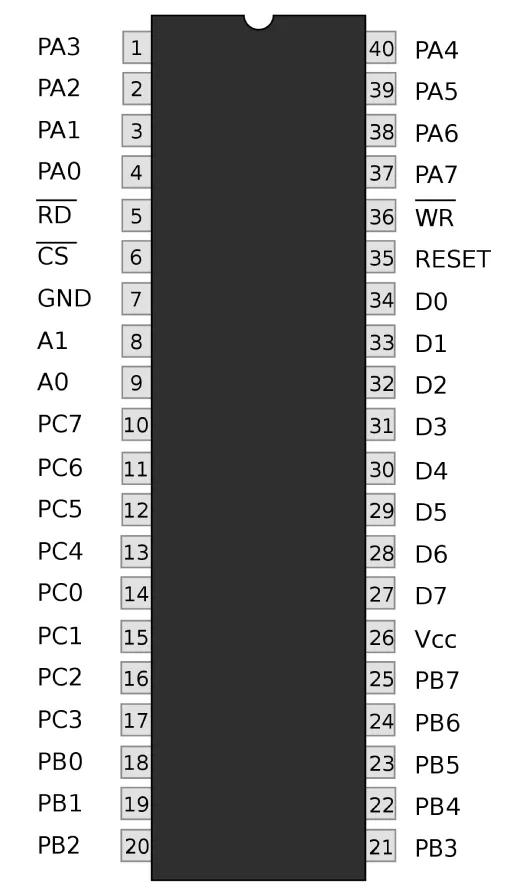
PA7 to PA0 (Port A Pins)
The PA7 to PA0 pins, occupying pins 1 to 4 and 37 to 40, represent the Port A data lines of the 8255 Microprocessor. Positioned evenly on both sides at the top of the microprocessor, these eight port A pins function either as buffered input lines or latched output lines, contingent upon the control word loaded into the control word register.
PB0 to PB7 (Port B Pins)
The PB0 to PB7, spanning from pins 18 to 25, constitute the data line pins responsible for transmitting port B data.
PC0 to PC7 (Port C Pins)
The PC0 to PC7 pins, located at pins 10 to 17, form the port C pins, carrying the port A data bits. Within this range, pins 10 through 13 are designated as Port C upper pins, while pins 14 through 17 are referred to as lower pins. These pins can be independently utilized to transmit 4 data bits each, effectively creating two separate segments of the port C.
D0 to D7 (Data Bus Pins)
Occupying pins 27 to 34, the D0 to D7 pins serve as data I/O lines, tasked with carrying the 8-bit binary code essential for the proper functioning of the entire integrated circuit. Collectively, these pins comprise the control register/control word, housing the necessary data for control operations.
A0 & A1
At pins 8 and 9, A0 and A1 play a decisive role in determining the preferred port for data transmission:
- A0 = 0 & A1 = 0: Port-A is selected.
- A0 = 0 & A1 = 1: Port-B is selected.
- A0 = 1 & A1 = 0: Port-C is selected.
- A0 = 1 & A1 = 1: The control register is selected.
CS’
Pin 6, labeled CS’, serves as a chip select input, responsible for activating a specific chip. A low signal at the CS’ pin enables communication between the 8255 and the processor, allowing data transfer operations to proceed upon receipt of an active low signal.
RD’
Pin 5, designated as RD’, serves as a read input pin, placing the chip into a read mode. A low signal at the RD’ pin facilitates the transfer of data from the chip to the CPU through a data buffer.
WR’
Similarly, pin 36, denoted as WR’, serves as a write input pin, initiating the chip's writing mode. Consequently, a low signal at the WR’ pin enables the CPU to execute write operations across the ports or the microprocessor’s control register via the data bus buffer.
RESET
Likewise, pin 35, known as the RESET pin, triggers a complete reset of all data stored within the keys to their default values when activated. Operating as an active high signal, a high signal at the RESET pin clears the control registers, placing the ports into input mode.
GND
Pin 7 serves as the ground (GND) pin of the IC.
VCC
On the other hand, pin 26, labeled as VCC, acts as the 5V input pin of the IC.
8255 Microprocessor Architecture
The architecture of the 8255 microprocessor is depicted below.
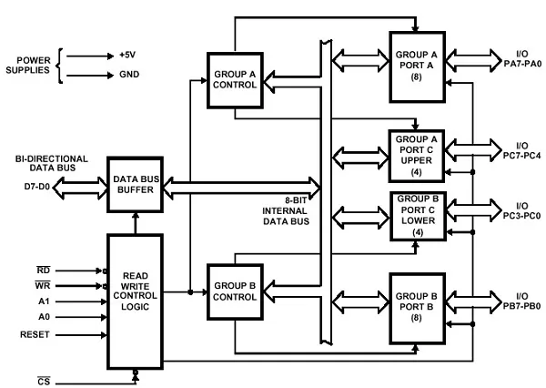
Architecture
Internal Bus Interface:
The internal bus interface serves as a crucial link between the microprocessor's internal bus and the system bus, facilitating seamless interfacing between the two. This interface enables read and write operations to and from the CPU, allowing data transmission between the control register or ports and the CPU during write operations, and between the CPU and the status register or ports during read operations.
Control Logic for Read/Write Operations:
Responsible for managing internal system operations, the control logic unit oversees both data transfers and the handling of status or control words internally and externally. When data retrieval is required, this unit prompts the generation of commands to the two control groups based on the address provided by the 8255 via the bus.
Control Groups A & B:
Both control groups, A and B, are under the jurisdiction of the CPU and operate according to commands issued by the CPU. Control words are transmitted from the CPU to these groups, which then relay the appropriate commands to their respective ports. Group A governs port A using higher-order port C bits, while Group B oversees port B with lower-order port C bits.
Port A & Port B:
Port A and Port B each feature an 8-bit input latch and 8-bit buffered or latched output, serving versatile functions regardless of the mode of operation. Port A can be configured in three modes: modes 0, 1, and 2, whereas Port B can be programmed in modes 0 and mode 1.
Port C:
Comprising an 8-bit data input buffer and an 8-bit bidirectional data output latch or buffer, Port C is divided into two main sections: Port C Upper (PCU) and Port C Lower (PCL). These sections can be programmed separately and are utilized as 4-bit I/O ports. Port C is instrumental for handshake signals, Simple I/O, and status signal inputs, often employed in conjunction with Port A and Port B for managing both status and handshake signals. Additionally, this port provides direct bit setting or resetting capabilities.
8255 Microprocessor Operating Modes
The 8255 microprocessor offers two distinct operating modes: the bit set-reset mode and the input/output mode, each detailed below.
Bit Set-Reset Mode
The bit set-reset mode primarily focuses on setting or resetting individual bits within Port-C. In this mode, only one bit of Port C is affected at a time, remaining set until manually unset by the user. To modify a bit, the user must load the desired bit pattern into the control register. Once Port C is designated for status or control operations, individual bits of Port C can be set or reset by sending an OUT instruction.
I/O Mode
The I/O mode comprises three variations: Mode 0, Mode 1, and Mode 2, each serving specific purposes elucidated as follows:
Mode 0:
Mode 0 is an I/O mode of the 8255 microprocessor that allows programming of each port as either an input or output port. Key features of this mode include:
- Buffered input ports with latched outputs.
- Absence of interrupt capability or handshaking.
Mode 1:
Mode 1 of the 8255 microprocessor entails I/O with handshaking, wherein both Port A and Port B function as I/O ports, while Port C is utilized for handshaking purposes. This mode facilitates synchronization of data transfer between devices operating at varying speeds. Inputs and outputs are latched, and the mode supports interrupt handling and signal control to synchronize CPU and IO device speeds.
Mode 2:
Mode 2 represents a Bidirectional I/O port with handshaking. In this mode, ports can facilitate bidirectional data flow through handshaking signals. Group A pins can be programmed for bidirectional data bus operation, while PC7 to PC4 in Port C are utilized for handshaking. The remaining lower bits of Port C are allocated for input/output operations. This mode also supports interrupt handling.
Working of 8255 Microprocessor
The operational principles of the 8255 microprocessor involve its role as a versatile programmable I/O unit primarily aimed at facilitating the transfer of information from input/output sources to interrupt-driven I/O when specific conditions dictate. Compatible with a wide range of microprocessors, this unit boasts three bidirectional I/O ports, namely PORT A, PORT B, and PORT C, configurable according to specific needs. The 8255 PPI is specifically engineered to establish connections between the CPU and external peripherals such as keyboards, ADCs, and DACs, its programmability enabling tailored functionality in response to defined conditions.
Interfacing 8255 PPI with 8086:
The integration of the 8255 PPI with the 8086 microprocessor is necessitated by the latter's activation of the input RD pin of the 8255 when data retrieval from an 8255 port is required. This RD pin operates on an active low logic, directly linked to the WR output of the 8086 microprocessor. Conversely, the WR input of the 8255 is triggered by the 8086 microprocessor when data writing to an 8255 port is initiated.
Data transfer between the 8255 and the 8086 microprocessor occurs via an 8-bit data bus, employing a serial communication protocol for efficient interaction. The internal configuration of the 8255 is controlled by utilizing address lines A1 and A0, facilitating precise selection of functions. Connection between the data bus pins (D0 to D7) of the 8255 and the data lines of the 8086 microprocessor is established, while read input pins (RD') and write input pins (WR') of the 8255 are linked respectively to the I/O read and I/O write functionalities of the 8086.
The 8255 features four primary ports—PA, PB, PC, and the control word—dedicated to data transmission, with the control word responsible for signaling. Two essential signals, namely the I/O signal and the BSR signal, are transmitted to the 8255. The I/O signal initializes the mode and direction of the ports, whereas the BSR signal facilitates the manipulation of signal lines for setting and resetting purposes.
In scenarios involving connected input devices, the device first seeks authorization from the PPI before proceeding with data transmission.

The 8255 PPI facilitates the transmission of data from input devices only when there is no pending data within the 8255 awaiting transmission to the 8086 processor. If the 8255 PPI retains any previously queued data, it refrains from permitting the input device to proceed.
Upon authorization by the 8255 PPI, data is acquired and temporarily stored in the PPI's registers. When data is present within the 8255 PPI and needs to be transferred to the 8086 processor, a signal is dispatched to the PPI.
Upon the 8086 processor becoming available to receive the data, it signals back, initiating the data transfer between the 8255 and the 8086. If the 8086 processor remains unavailable for an extended period, indicating that the 8255 PPI still holds untransmitted data, the input device is prohibited from transmitting further data to prevent data loss due to potential overwriting. The curved arrow signal depicted in the diagrams signifies the handshake signal, thereby dubbing this data exchange process as handshaking.
Considerations for Interfacing with the 8255 Microprocessor
Various aspects require attention when interfacing with the 8255 microprocessor, as outlined below.
In its unprogrammed state, the 8255 ports function as input ports. If configured as output ports in this state, connecting an input device would result in both the input device and the 8255 producing outputs on the port lines, potentially causing interference or damage to either or both devices.
The output pins of the 8255 lack the capacity to power external devices due to insufficient driving current.
When connecting devices such as motors, lamps, or speakers to the 8255, it's crucial to verify the current rating of both the devices and the 8255 to ensure compatibility.
In scenarios where the 8255 cannot supply adequate driving current, the use of inverting amplifiers like the 7406 and noninverting amplifiers like the 7407 is recommended. For applications with high current demands, transistors configured in a Darlington Pair arrangement can be employed.
When interfacing a DC motor with the 8255, selecting suitable H-Bridges based on the motor specifications is essential, as H-Bridges enable a DC motor to operate in both directions.
Port A and Port B are restricted to 8-bit functionality, necessitating that all pins of these ports be designated as either input or output.
For AC-powered devices connected to the 8255, employing relays for protection is advisable.
Once Port A and Port B are programmed in Mode 1 or Mode 2, Port C loses its capability to function as a standard I/O port.
Q: How is the 8255 Microprocessor interfaced with the main processor?
A: The 8255 Microprocessor is connected to the main processor through an address bus and a data bus. The main processor communicates control signals and directives to the 8255 Microprocessor via the data bus, while data transmission between the two occurs bidirectionally through the data bus.
Q: What are the three operational modes available in the 8255 Microprocessor?
A: The 8255 Microprocessor offers three distinct operational modes:
Mode 0: Fundamental Input/Output mode
Mode 1: Controlled Input/Output mode
Mode 2: Dual-directional bus mode
Q: How does the 8255 Microprocessor manage interrupts?
A: The 8255 Microprocessor is equipped to trigger interrupts upon the satisfaction of specific input or output conditions. These interrupts can be programmed to activate on designated ports or specific bits within a port. Upon interrupt occurrence, the main processor executes a predefined interrupt service routine.
Q: What are the practical applications of the 8255 Microprocessor?
A: During the 1980s, the 8255 Microprocessor found extensive utilization in furnishing parallel input/output capabilities to various microprocessors. Its applications spanned diverse fields including data acquisition, process control, and industrial automation.
Q: How does the 8255 Microprocessor oversee handshake signals?
A: Incorporating built-in handshake signal generation functionality, the 8255 Microprocessor can both generate and respond to an array of handshake signals such as READY, ACK, and BUSY. These signals serve to regulate the data flow between the main processor and the 8255 Microprocessor.
Q: Is the 8255 Microprocessor still utilized today?
A: The 8255 Microprocessor is considered outdated and is no longer manufactured. Nonetheless, it still sees occasional use in legacy systems or projects necessitating parallel input/output capabilities. Presently, there exist more modern and sophisticated peripheral interface chips capable of fulfilling the same tasks as the 8255 Microprocessor.
The 8255 Microprocessor is deemed obsolete in contemporary contexts and is no longer being produced. Alternative peripheral interface chips with enhanced functionalities have emerged to supplant the role of the 8255 Microprocessor.
An instance of such a substitute is the 8255A, designed as a drop-in replacement for the 8255 while incorporating additional features and enhancements.
Another alternative is the 8254 Programmable Interval Timer, serving as a programmable timer and counter chip suitable for systems requiring precise timekeeping and event counting, thereby offering a replacement option for the 8255.
Moreover, modern microcontrollers like Arduino or Raspberry Pi can be programmed to execute the same input/output operations as the 8255 while providing extended functionalities.
Furthermore, an array of general-purpose input/output (GPIO) chips, such as the 74HC595, MCP23017, and PCF8574, offer parallel input/output capabilities, albeit with potential compatibility discrepancies with the 8255, necessitating software and/or hardware adaptations for seamless integration as replacements.
Advantages:
The benefits of the 8255 Microprocessor encompass the following:
- Compatibility: The 8255 Microprocessor is compatible with nearly all microprocessors.
- Versatility: Various ports can be configured to serve as input/output functions.
- Power Efficiency: It operates efficiently with a regulated +5V power supply.
- Popularity: Widely utilized as a coprocessor, the 8255 enjoys widespread adoption.
- Interface Functionality: Serving as an interface between the microprocessor and peripheral devices, the 8255 facilitates the parallel transfer of data.
Applications:
The applications of the 8255 Microprocessor span diverse domains, including:
- Peripheral Connectivity: Used for linking peripheral devices with interfaces such as LED or Relay Interface, Stepper Motor Interface, Display Interface, Keyboard Interface, ADC or DAC Interface, Traffic Signal Controller, and Lift Controller.
- Programmable Interface: Renowned as a programmable peripheral interface device, the 8255 finds extensive application.
- Data Transmission: Employed in transmitting data across various operational conditions.
- Motor Interface: Utilized for interfacing with both stepper motors and DC motors.
- Microcontroller Systems: Widely integrated into microcontroller and microcomputer systems, including home computers such as all MSX models and the SV-328.
- Computer Compatibility: Compatible with original PC/XT, IBM-PC, PC/jr, and clones, as well as in conjunction with various homebuilt computers like the N8VEM.
Hence, this provides an overview of the 8255 Microprocessor, covering its architecture, functionality, and applications. The 82C55 Microprocessor serves as a versatile programmable I/O unit, compatible with a multitude of microprocessors. Employing an industry-standard setup, the high-performance 82C55 Microprocessor seamlessly integrates with the 8086. Now, let me pose a question: What exactly is an 8086 microprocessor?
Related Articles
Microprocessor Vs Integrated Circuit: What’s the Differences?


