


FinFET vs MOSFET: Which Transistor Should You Choose?
Introduction
Comparison of FinFET vs. MOSFET is one of the most significant changes in contemporary semiconductor device engineering, and it can be said that the development of the transistor structure was aimed at overcoming the physical scaling limitations of a transistor-like device, preserving its performance, power usage, and reliability. Plane-based MOSFETs had been at the backbone of integrated circuits and allowed the Moore Law to shape an exponential growth in computing capacity; however, as feature sizes neared the deep submicron level, leakage current and short-channel effects, in addition to electrostatic control constraints, became critical. FinFET technology was a structural instead of a material innovation, where the channel of the transistor was redesigned in three dimensions to again provide access to the gate control and allow further scaling. Knowledge of the differences between FinFET and MOSFET is crucial to the IC designer, system designer, and component engineer who need to trade off between performance, cost, power consumption, and manufacturability when choosing transistor technologies.
What Is a MOSFET?
Metal-Oxide-Semiconductor Field-Effect Transistor (MOSFET) is an electrically manageable semiconductor device in which current flows through the planar channel at the semiconductor face, because of an electric field by means of the gate electrode. The oxide layer, which surrounds the gate and the channel, is thin, thus making the MOSFET of high input impedance and low level of static power consumption. Planar MOSFETs were used in digital and analog circuits since they can be scaled, integrated into CMOS processes, and used in large and small-scale voltage and current ratings, such as small-signal logic transistors and high-power discrete components.
Types of MOSFETs
MOSFETs are broadly classified into NMOS and PMOS devices based on carrier type, as well as enhancement-mode and depletion-mode variants depending on whether a channel exists at zero gate bias. In integrated circuits, CMOS logic is based on complementary NMOS and PMOS transistors, which reduce the amount of power dissipation when at rest, whereas in power electronics, the vertical power MOSFET is optimized with low on-resistance and large current density. Although structurally different, planar MOSFETs are all based on two-dimensional channels created parallel to the silicon surface.
Key Electrical Characteristics of MOSFETs
The electrical behavior of a MOSFET is defined by parameters such as threshold voltage, channel mobility, drain-induced barrier lowering (DIBL), subthreshold slope, and on-resistance. As MOSFET dimensions shrink, electrostatic control weakens, leading to increased leakage current, threshold voltage roll-off, and variability, which significantly impact power efficiency and yield in advanced nodes.
What Is a FinFET?
A FinFET (Fin Field-Effect Transistor) is a non-planar MOSFET design with the channel created in thin vertical silicon fins sticking out of the substrate, leaving the gate the possibility of encircling several sides of the channel. This three-dimensional architecture is a vast enhancement of the electrostatic control of the channel, reducing leakage current and allowing lower operating voltages in advanced technology nodes. At the 22 nm node and smaller, FinFETs became generic in commercial manufacturing and represented a radical change in the design of transistors as opposed to scale.
FinFET Structure and Working Principle
In contrast to the planar type of MOSFET, where the gate is able to control a channel on one side, a FinFET gate normally encircles the fin on three sides, forming a tri-gate structure that increases the gate-to-channel coupling. By making sure that the channel potential curve is dominated by the gate as opposed to the drain, this geometry, which also has short-channel suppression, has the effect of obtaining steeper subthreshold slopes and better on/off current ratio.
Common FinFET Variants
The implementation of FinFETs differs among foundries, with bulk FinFET allotment of conventional silicon material and SOI-based FinFETs, which have additional benefits of isolation. Variants can be based on either a double-gate or tri-gate, depending on the fin height and process optimization, although they all operate on the same principle of multi-gate electrostatic control.
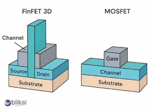
FinFET vs MOSFET: Structural Differences
The basic structural distinction between FinFET and MOSFET is the channel geometry and the positioning of the gate with planar MOSFETs having a flat, surface-based channel with the gate being controlled by an attractive surface from above, and FinFETs having a vertical fin with the gate being placed on each side. This architecture will convert the two-dimensional structure of the transistor into a quasi-three-dimensional structure, which explicitly overcomes the scaling limitations, manifested by planar MOSFETs at small gate lengths. The increased effective channel width per footprint in FinFETs also allows higher drive current without proportional area scaling.
FinFET vs MOSFET: Electrical Performance Comparison
FinFETs also have superior drive current, low subthreshold slope and much lower leakage current than planar MOSFETs of the same technology node. The gate control of FinFETs allows reduced supply voltages with similar performance to superior performance, and thus is applicable in high-speed, low-power digital circuits. Planar MOSFETs, while still effective at larger geometries, suffer from degraded off-state behavior and reduced scalability below approximately 20 nm.
Power Efficiency and Thermal Characteristics
One of the main benefits of FinFET technology is power efficiency because minimized leakage current corresponds to minimized static power consumption in large-scale integrated circuits. Nevertheless, the thermal characteristics of FinFETs are more problematic because thermal diffusion processes are restricted compared to those in planar devices, and thermal design must be done at both chip and package levels. Planar MOSFETs, particularly in discrete power applications, often offer superior thermal performance due to larger junction areas and simpler heat spreading.
Manufacturing Complexity and Cost Considerations
The fabrication process of FinFET is much more complicated than that of planar MOSFET manufacturing, which requires sophisticated lithography, fine etching of the fins, and strict control of dimensions, so that they achieve homogenous electrical properties. These demands raise the cost of capital and cost of process, and FinFETs are only economical in high-volume, high-performance ICs. Enhanced by this is that planar MOSFETs have mass-produced, low-cost processes, which are also appealing to legacy nodes, analog circuits and power devices that do not need extreme scaling.
Scalability and Technology Node Limitations
Planar MOSFETs face fundamental electrostatic limitations as gate lengths shrink, leading to unacceptable leakage and variability, while FinFETs extend scalability by enhancing gate control without requiring prohibitively thin gate oxides. Nevertheless, scaling FinFETs is problematic at smaller sizes, around 3 nm, and the industry is considering the next evolutionary step to FinFETs to be a gate-all-around (GAAFET) architecture or a nanosheet architecture.
Reliability and Variability Considerations
Reliability factors such as bias temperature instability, hot carrier injection, and process-induced variability affect both FinFETs and MOSFETs, but the stronger electrostatic control of FinFETs generally improves tolerance to short-channel-induced degradation. At the same time, FinFETs are more sensitive to geometric variations in fin width and height, making process control and design margin critical for yield and long-term stability.
Typical Applications of MOSFETs
MOSFETs remain indispensable in discrete power electronics, automotive systems, industrial control, and analog circuits, where voltage and current handling, cost efficiency, and thermal robustness are prioritized over extreme scaling. Planar MOSFETs have found many applications in motor drives, DC-DC converters and switching regulators, and clearly indicate that planar MOSFET technology remains a critical component outside the advanced digital IC nodes.
Typical Applications of FinFETs
FinFETs dominate advanced logic ICs, including CPUs, GPUs, mobile SoCs, AI accelerators, and high-performance computing processors, where power efficiency and transistor density are critical. They are the optimal choice of transistor architecture for the state of the art semiconductor processes for battery-powered and thermally-constrained systems, as well as in thermally-constrained systems which need high performance at low supply voltages.
FinFET vs MOSFET: Which Should You Choose?
FinFET or MOSFET is a decision that varies according to the requirements of the application, manufacturing constraints, and desired performance, with FinFETs being favored in the implementation of advanced digital logic at the small node scale and MOSFETs being preferable in the implementation of cost-sensitive, high-voltage or discrete applications. Instead of considering the two technologies as direct substitutes, designers have to consider trade-offs in terms of power consumption, scalability, process availability, and the overall system cost.
Future Trends: Beyond FinFET and MOSFET
With further semiconductor scaling, FinFETs will be replaced by gate-all-around and nanosheet transistors that will provide even better electrostatic control and scalability. However, the simplicity, reliability and economic benefits of planar MOSFETs will continue to be found in various fields of application, meaning that there will be several transistor architectures that exist throughout the semiconductor industry.
FAQ
Is FinFET replacing MOSFET completely?
FinFET is not replacing MOSFET entirely; instead, it replaces planar MOSFETs only in advanced logic nodes where scaling limitations demand better electrostatic control, while planar MOSFETs remain widely used in power, analog, and mature-node applications.
Why does FinFET consume less power than MOSFET?
The lower power consumption of FinFETs is mainly due to the fact that the multi-gate structure of FinFETs lowers leakage current and allows lower operating voltages without compromising performance.
Are FinFETs used in discrete electronic components?
FinFETs are rarely used in discrete components due to cost and manufacturing complexity, with most discrete transistors continuing to use planar or vertical MOSFET structures.
Can MOSFETs still be used in advanced ICs?
Planar MOSFETs are generally unsuitable for advanced nodes below ~20 nm due to short-channel effects, but they are still used in mixed-signal and peripheral circuits within advanced chips.
What comes after FinFET technology?
The successors to FinFETs are regarded as gate-all-around and nanosheet transistors, which will provide an even better scalability and performance in the upcoming semiconductor nodes.
Conclusion
The FinFET and MOSFET technologies play different roles in modern electronics, which are characterized by different priorities of performance, power use, costs and scalability. Knowing their structural, electrical, and manufacturing differences, engineers and decision-makers can be able to choose the most suitable transistor architecture to use in their particular application in order to have a good balance between innovation and feasibility.
Some images are sourced online. Please contact us for removal if any copyright concerns arise.


