


CD4035 Shift Register: Features, Specifications and Applications
Digital shift registers, such as the CD4035, are widely used digital integrated circuits, known for their efficient data storage and transfer functionality. Shift registers belong to the CMOS family, which are designed for high-speed, low-power operations. It is widely used in applications such as data manipulation, signal processing, and microcontroller interfacing because of its ability to shift data in multiple modes. CD4035 shift registers are discussed in this introduction, which highlights their significance in modern electronics through their key features, technical specifications, and practical applications.
What is CD4035 Shift Register?
CD4035 is a 3-bit parallel-in/4-bit parallel-out shift register CMOS (Complementary Metal-Oxide Semiconductor). In addition to storing and transferring data quickly, it consumes little power, making it ideal for a wide range of digital applications. Shift registers are multistage devices that can operate in serial and parallel modes. Each stage can hold a bit of data. Digital systems requiring precise control and timing rely on this ability to manipulate data, such as shifting, loading, and storing binary data.
In applications such as digital signal processing, communication systems, and microcontroller interfacing, the CD4035 can shift data left or right to enable efficient data handling and processing. Besides the asynchronous reset and clock enable inputs, the shift register also includes additional functionality for increasing data flow control and versatility. CD4035's robust performance and adaptability make it an ideal component for designing complex digital circuits with reliable operating characteristics and easy integration.
Features
4-Bit Shift Register
Shift registers such as CD4035 are 4-bit devices, which means four bits can be stored and shifted simultaneously. Binary numbers are represented by four bits (0 or 1), each of which represents a binary digit (0 or 1). Small amounts of data can be stored and manipulated in digital circuits using this capability. It is ideal for simple data processing tasks and compact digital designs due to its 4-bit structure, which allows efficient data handling.
Parallel-In/Parallel-Out Functionality
The CD4035 features a parallel-in/parallel-out function that sets it apart from other products. Four bits can be accepted simultaneously and output in parallel. Data can be transferred quickly between circuit parts when using this feature. It enables microcontrollers to load and retrieve data more quickly, enhancing the overall performance of the system. By handling data in parallel, circuits requiring synchronized operations can be designed more easily.
Serial Data Shifting
Besides parallel data handling, the CD4035 also handles serial data, either left or right. Data serialization, where parallel data needs to be converted into a serial stream for communication purposes, makes use of serial shifting to move data bits one position per clock cycle. The ability to transmit data over single lines is especially useful in communication systems, where fewer connections are required. In digital signal processing, serial shifting is also useful for implementing algorithms that are based on bit-wise data manipulation.
Asynchronous Reset
Asynchronous reset inputs are provided on the CD4035, which enable immediate clearing of register data. Any bit in a shift register will be set to zero upon activating the reset input, regardless of the clock signal. Data operations can be started quickly by using this feature, or data can be cleared faster by responding to specific conditions in the circuit. Shift registers can be controlled more effectively and reliably with asynchronous resets.
Clock Enable Input
In addition to its clock enabled input, the CD4035 has other important features. Shift register response to clock pulses is controlled by this input. Shift registers respond to clock signals by shifting or loading data, when clock enable is enabled. A register holds its current state when the clock enable input is inactive. The shift register is synchronized with other parts of the circuit by allowing precise control over when data is shifted or loaded.
Low Power Consumption
In addition to its low power consumption, the CD4035 shift register uses CMOS technology. Consequently, the CD4035 is suitable for applications requiring high energy efficiency, such as battery-powered devices. Power consumption is also low, so the device will be more reliable and last longer. Especially in portable electronic devices, where battery life is an important consideration, this feature is extremely beneficial.
Wide Operating Voltage Range
Voltages ranging from 3V to 15V are supported by the CD4035. It can be used in a variety of environments and with different power supplies because of this flexibility. CD4035 is suitable for both low-voltage portable devices and higher-voltage industrial systems. Also, its wide voltage range simplifies the design and integration process in complex circuits, allowing a wider variety of other digital components to be integrated.
Robust Performance and Reliability
Known for its high reliability and robust performance, the CD4035 shift register offers high performance. Data can be processed and transferred quickly due to its high speed capabilities. A range of environmental conditions can be handled with ease, ensuring consistent performance regardless of the operating scenario. For critical applications such as industrial control systems and automotive electronics, such as those requiring consistent operation over time, this reliability is essential.
Specification
-
Number of Bits: 4 bits
-
Input Voltage Range: 3V to 15V
-
Output Voltage Range: 0V to VDD (up to 15V)
-
Input Current: ±1 µA (max)
-
Output Current: ±10 mA (max)
-
Power Dissipation: 500 mW (max)
-
Propagation Delay Time: 200 ns at 10V (typical)
-
Clock Frequency: Up to 10 MHz (depending on supply voltage)
-
Quiescent Current: 1 µA (max) at 5V
-
Operating Temperature Range: -55°C to +125°C
-
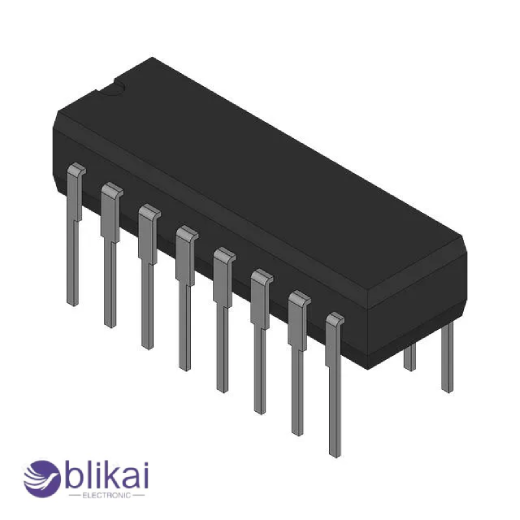
Package Types: DIP-16, SOIC-16, and TSSOP-16
-
Clock Input (CLK): Controls the shifting and loading of data
-
Parallel Data Inputs (P0-P3): For parallel data entry
-
Serial Data Inputs (SI, SO): For serial data entry and output
-
Asynchronous Reset (RST): Clears all register contents
-
Clock Enable (EN): Enables or disables the clock input
-
High Noise Immunity: Provides reliable operation in noisy environments
-
Low Power Consumption: Ideal for battery-powered and energy-efficient applications
Applications
Data Storage and Transfer
Data storage and transfer in digital circuits are commonly accomplished using the CD4035 shift register. This component is essential for managing data flow within a system due to the fact that it can hold and shift data in both parallel and serial formats. Data from sensors or other inputs can be temporarily stored in a shift register before being processed in microcontroller-based projects, for example. It reduces errors and improves the efficiency of the system by organizing data in a logical manner. A shift register's ability to transfer data serially simplifies communication between different parts of a circuit, especially when fewer connections are required.
Serial-to-Parallel and Parallel-to-Serial Conversion
Data conversion between serial and parallel formats is another key application of the CD4035. As a bridge between serial communication and parallel processing, the shift register acts as a means of transmitting data over a single line (serial communication). It is compatible with peripherals such as displays and other peripheral devices that operate via parallel inputs, such as communication modules, which can receive serial data. In embedded systems, it also converts parallel data from a microcontroller to a serial format and transmits it efficiently.
Signal Processing
Digital signal processing applications can benefit from the CD4035 shift register. Shift registers are useful in these scenarios since they can efficiently handle data manipulation in a specific sequence or order. Using a shift register, for example, you can delay audio signals by a certain number of clock cycles to create effects like echo. In both simple and complex applications, the CD4035 ensures accurate signal processing by shifting data through its stages and maintaining the desired timing and sequence.
Microcontroller Interfacing
The CD4035 can also be used to interface with microcontrollers. Shift registers can expand the I/O capabilities of microcontrollers with limited input/output (I/O) pins. A microcontroller, for example, can control multiple outputs by controlling a shift register. Projects involving several LEDs, switches, or other components that require individual control can benefit from this expansion. By utilizing more I/O pins without needing additional pins, the CD4035 optimizes the use of available resources on microcontrollers.
LED Display Control
LED displays are frequently controlled by the CD4035 shift register. A large number of output pins are required to manage multiple LEDs individually, which can be time-consuming. The shift register can drive LEDs in parallel by loading serial data into it and then outputting it in parallel. Wiring is simplified and microcontroller pins are reduced with this method. Displaying characters, numbers, or animations requires precise control of the LED segments in LED matrices or segmented displays.
Keyboard Encoding
Keypresses can be scanned and encoded using the CD4035 shift register in keyboard encoding applications. Shift registers can read signals generated by a pressed key. A microcontroller or processor can decode the serial data stream to determine which key was pressed by the register, which converts these signals into a serial data stream. Embedded systems often require reliable and efficient key press detection when creating custom keyboards for user interfaces.
Frequency Division
In addition to frequency division applications, the CD4035 can also be used. This can be accomplished by shifting the clock pulses through the stages of the shift register as it divides the frequency of the clock signal. A lower frequency signal can be generated from a high-frequency clock source using this divided frequency. Different types of electronic devices require frequency division to function properly, such as clocks, timers, and pulse generators.
Conclusion
Among the many versatile and reliable components found in digital electronics is the CD4035 shift register. Asynchronous reset and clock enable, as well as parallel and serial data handling capabilities, make it indispensable for a wide range of applications. With robust performance and ease of use, the CD4035 can handle a wide range of tasks, including data storage, signal processing, and microcontroller interfacing. A wide range of operating voltages and low power consumption further enhance the attractiveness of this device, ensuring dependable and efficient operation in a variety of environments. No matter what level of experience you have with digital circuits, the CD4035 shift register will prove valuable to you.
Related Articles
Discrete Circuit vs Integrated Circuits: What's the Differences?
Microprocessor vs Integrated Circuit:Which One Is Better
What is an Integrated Circuit (IC)? Working, and Types (Guide)
Microprocessor Vs Integrated Circuit: What’s the Differences?


