


What is Analog to Digital Converter & How it works
Nearly every measurable environmental parameter, such as temperature, sound, pressure, light, is in analog form. For example, in a temperature monitoring system that requires acquiring, analyzing, and processing data from with digital computers and processors. Therefore, an intermediate device is necessary to convert the analog temperature data into digital format so can be communicated with digital processors like microcontrollers and microprocessors. The Analog to Digital Converter (ADC) is an electronic integrated circuit utilized for this purpose – it converts analog signals such as voltages into digital or binary form consisting of 1s and 0s. Many ADCs take a voltage input range of 0 to10V or -5V to +5V and produce corresponding digital output in the form of a binary number.
What is an Analog to Digital Converter?
An Analog to Digital Converter, also known as ADC converter, is a device used to convert analog signals into digital form. This type of converter takes the signal from continuous form and converts it into discrete form. It can be referred to as A/D, ADC or A to D. The converse of a DAC is an ADC. The symbol for an analog to digital converter is depicted below.
The conversion of an analog signal into digital format can be achieved through various methods. There are numerous types of ADC chips on the market from different manufacturers such as the ADC08xx series. Hence, a basic ADC can also be constructed using discrete components.
The primary characteristics of an ADC are its sample rate and bit resolution.
The sample rate refers to how quickly an ADC can convert a signal from analog to digital form.
Bit resolution indicates the level of accuracy with which an analog to digital converter can convert the signal from analog to digital.
One of the key advantages of an Analog to Digital Converter (ADC) is its ability to achieve a high data acquisition rate, even with multiplexed inputs. The availability of a wide range of ADC integrated circuits (ICs) has enhanced the accuracy and speed of data acquisition from different sensors. High-performance ADCs exhibit improved measurement repeatability, low power consumption, precise throughput, high linearity, and excellent Signal-to-Noise Ratio (SNR), among other dynamic characteristics.
ADCs find application in various fields such as measurement and control systems, industrial instrumentation, communication systems, and all other sensor-based systems. These converters can be classified based on factors such as performance, bit rates, power consumption, cost considerations, etc.
ADC Block Diagram
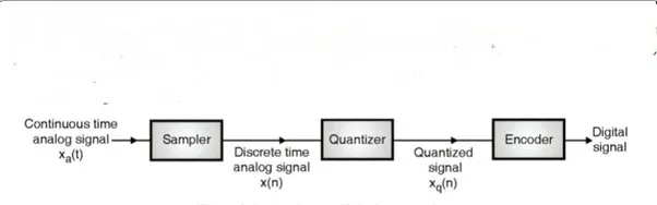
Below is the block diagram of an Analog to Digital Converter (ADC), which consists of a sample, hold, quantize, and encoder. The process of ADC can be understood as follows.
Initially, the analog signal is inputted into the first block, known as a sample, where it is sampled at a specific sampling frequency. The amplitude value of the sample, as an analog value, is then held within the second block called Hold. Subsequently, the held sample is quantized into discrete values through the third block known as quantize. Lastly, in the encoder stage, these discrete amplitudes are converted into binary numbers.
The above block diagram illustrates how ADC converts signals from analog to digital form.
Sampling
In the sample block, the analog signal is taken at specific intervals of time. The samples retain continuous amplitude and real value, but they are discrete in terms of time. The sampling frequency plays a crucial role in accurately maintaining this rate and can be set according to system requirements.
Hold
The second block in an ADC, HOLD, serves as a buffer that holds the sample amplitude until the next sample is taken. The value of hold remains unchanged until the next sample.
Quantize
In ADC, this third block is primarily used for quantization. Its main function is to convert continuous (analog) amplitude into discrete values. The continuous amplitude value held within the hold block moves through the quantize block to become discrete in amplitude. As a result, the signal then exists in digital form with discrete amplitudes and time components.
Encoder
The final block in an ADC is the encoder, which converts the signal from digital form to binary. As we know, digital devices operate using binary signals, so it is necessary to convert the signal from digital to binary using an encoder. This completes the process of converting an analog signal to digital using an ADC. The entire conversion process can be completed within a microsecond.
Analog to Digital Conversion Process
There are various methods for converting analog signals into digital signals. These converters have numerous applications as intermediate devices for converting signals from analog to digital form and displaying output on LCDs through microcontrollers. The objective of an A/D converter is to determine the output signal word that corresponds to an analog signal. Now let's explore the ADC 0804, which is an 8-bit converter with a 5V power supply and can accept only one analog input signal.
The digital output ranges from 0 to 255 in an ADC. It requires a to function, and the time it takes to convert the analog to digital value is dependent on the clock source. An external clock can be provided to pin no. 4, CLK IN. To use the internal clock, a suitable RC circuit is connected between pins CLK IN and CLK R. Pin 2 serves as the input pin – bringing data from the internal register to the output after conversion when a high-to-low pulse is applied. Pin 3 acts as Write – providing a low-to-high pulse for an external clock input. Pins 11 through 18 are data pins from Most Significant Bit (MSB) to Least Significant Bit (LSB).
In an Analog to Digital Converter, each falling or rising edge of the sample clock triggers sampling of the analog signal. During each cycle, the ADC acquires, measures, and converts this analog signal into a digital value with fixed precision.
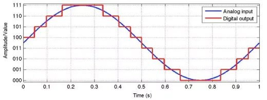
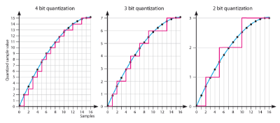
The accuracy of capturing original analog signals in ADCs depends on two factors: quantization level or bit and sampling rate. The resolution of digitized output is determined by bit rate; for example, in Figure below where a 3-bit ADC is used for converting an analog signal.
The image below illustrates how analog-to-digital conversion occurs.
If we are using a 3-bit ADC to convert a one-volt signal, then there are 2^3=8 divisions available for generating the 1V output. This means that each division represents a minimum change, or quantization level, of 1/8=.125V. These levels are represented as follows: 000 for V, 001 for .125V, and so on up to 111 for 1V. Increasing the bit rate to values such as 6,8,12 or16 will result in better precision of the signal. Therefore, the bit rate or quantization determines the smallest change in analog signal value resulting from a change in digital representation.
For example, if we have an input signal ranging from -5V and we use an8-bit ADC then the binary output for5Vis256.
There is an absolute chance of misrepresenting the input signal on the output side if it is sampled at a different frequency than the desired one. Therefore, another important consideration of the ADC is the sampling rate. The Nyquist theorem states that the acquired signal reconstruction introduces distortion unless it is sampled at (minimum) twice the rate of the largest frequency content of the signal as you can observe in the diagram. But this rate is 5-10 times the maximum frequency of the signal in practice.
Evaluation of ADC Performance
Various factors contribute to the evaluation of ADC performance, with two main factors detailed below:
Signal-to-Noise Ratio (SNR)
SNR measures the average number of noise-free bits in a specific sample.
Bandwidth
The sampling rate determines the bandwidth of an ADC, as it allows for discrete value production from the analog source per second.
Types of Analog to Digital Converters
Different types of ADCs are available, including:
- 1. Dual Slope A/D Converter
- 2. Flash A/D Converter
- 3. Successive Approximation A/D Converter
- 4. Semi-flash ADC
- 5. Sigma-Delta ADC
- 6. Pipelined ADC
Dual Slope A/D Converter Operation:
This type generates a comparison voltage using an integrator circuit constructed with a combination of resistor, capacitor, and operational amplifier components. The integrator produces a sawtooth waveform on its output from zero to Vref based on the set value of Vref. As the integrator waveform commences, the counter begins counting from to 2^n-1 where n represents the number of bits in the ADC's output.
When the input voltage Vin matches the waveform voltage, the control circuit records the counter value, which represents the digital value of the corresponding analog input. The Dual Slope ADC is a relatively affordable and slow device.
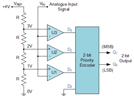
Flash A/D Converter
Also known as a parallel ADC, this converter IC is widely used for its speed. The flash analog-to-digital converter circuit consists of several comparators, each comparing the input signal with a unique reference voltage. Each comparator outputs a high state when the analog input voltage exceeds its reference voltage. The output is then sent to a priority encoder to generate binary code based on higher-order input activity while disregarding other active inputs. This flash type is a high-cost and high-speed device.
Successive Approximation A/D Converter
The SAR ADC is a more advanced ADC that is faster than dual slope and flash ADCs. It uses digital to approximate the closest value to the analog input voltage. This circuit includes a comparator, output latches, successive approximation register (SAR), and D/A converter.
Initially, the SAR is reset and as the LOW to HIGH transition occurs, the MSB of the SAR is set. The output is then sent to the D converter, which produces an analog equivalent of the MSB that is compared with the analog input Vin If the comparator output is LOW, then the SAR clears the MSB; otherwise, it sets it to the next position. This process continues until all bits are tested and Q0, valid data is present on the parallel output lines.
Semi-flash ADC
These types of analog-to-digital converters overcome their size limitations by using two separate flash converters. Each converter has half of the resolution bits for this semi-flash device. One flash converter handles most significant bits (MSBs) while another handles least significant bits (LSBs).
Sigma-Delta ADC
Sigma Delta ADCs (ΣΔ) are a relatively new design. They are slower compared to other designs but offer maximum resolution for all types of ADCs. They are commonly used in high-fidelity audio applications but not typically suitable for high bandwidth requirements.
Pipelined ADC
Pipelined ADCs, also known as sub-ranging quantizers, have a concept similar to successive approximations but are more sophisticated in approach. Rather than going through each step by moving to next MSB like successive approximations do,this type of ADC uses a different process:
- 1. Coarse conversion: Used as an initial conversion.
- 2. Evaluation: Determines change towards input signal.
- 3.Temporary Conversion: Allows for conversion with a range of bits.
Pipelined designs generally strike a balance between SAR and flash analog-to-digital converters in terms of size, speed, and resolution capabilities.
Examples of Analog to Digital Converters
Here are some examples of analog to digital converters:
ADC0808
The ADC0808 is a converter that has 8 analog inputs and 8 digital outputs. It enables the monitoring of up to 8 different transducers using a single chip, eliminating the need for external adjustments.
This monolithic CMOS device offers high speed, high accuracy, minimal temperature dependence, excellent long-term accuracy and repeatability, and consumes minimal power. These features make it suitable for applications ranging from process and machine control to consumer and automotive applications. The pin diagram of ADC0808 is depicted in the figure below:
Features:
- - Easy interface with all microprocessors
- - No zero or full-scale adjustment required
- - 8-channel multiplexer with address logic
- - Input range from V to 5V with single 5V power supply
- - Outputs meet TTL voltage level specifications
- - Carrier chip package with 28 pins
Specifications:
- - Resolution: 8 Bits
- - Total Unadjusted Error: ±½ LSB and ±1 LSB
- - Single Supply: 5 VDC
- - Low Power: 15 mW
- - Conversion Time: 100 μs
Generally, the input to be converted into digital form can be selected by using three address lines A, B, C (pins 23,24,and25). The step size depends on the set reference value. Step size refers to the change in analog input needed for a unit change in the output of ADC. Unlike ADC0804 which has an internal clock, ADC0808 requires an external clock signal.
The continuous output is an eight-bit digital representation corresponding to the instantaneous value of the analog input. The maximum level of input voltage must be reduced proportionally within +5V.
The ADC0808 IC operates with a clock signal typically at around550 kHzand is used for converting data into digital form as required by microcontrollers.
Applications of the ADC0808
The ADC0808 has a wide range of applications; here are some examples:
- In the circuit below, the clock, start, and EOC pins are connected to a microcontroller. Although there are 8 inputs available, only 4 inputs are utilized in this operation.
- The LM35 temperature sensor is connected to the first 4 inputs of the analog to digital converter IC. The sensor has three pins: VCC, GND, and output. When the sensor is heated, the voltage at the output increases.
- The address lines A, B, C are connected to the microcontroller for issuing commands. In this setup, interrupts occur on a low-to-high transition.
- When the start pin is held high, no conversion takes place. However, when it is set low,the conversion begins within 8 clock periods.
- Once conversion is complete,the EOC pin goes low to indicate thattheconversion process has finishedandthe data is ready for retrieval.
- The output enables (OE) signalis then raised high.This activates TRI-STATE outputs and allows data reading.
As we all know, analog-to-digital converters (ADCs) are widely used for converting analog signals into digital numbers to facilitate reading by microcontrollers. Among the various ADC models available, such as ADC0801, ADC0802, ADC0803, and ADC0808, this article will focus on the ADC0804 converter.
The ADC0804 is an 8-bit analog-to-digital converter that is commonly utilized. It operates with an analog input voltage range of V to 5V and features a single analog input and 8 digital outputs. The conversion time is a critical aspect in evaluating an ADC; for the ADC0804 model, it cannot exceed 110 μs and varies depending on the clocking signals applied to the CLK R and CLK IN pins.
Pin Description of the ADC804
- - Pin 1: Chip select pin that activates the ADC when low
- - Pin 2: Input pin where a high to low pulse retrieves data from internal registers to output pins after conversion
- - Pin 3: Input pin where a low to high pulse initiates conversion
- - Pin 4: Clock input pin for external clock signal
- - Pin 5: Output pin that goes low when conversion is complete
- - Pin 6: Analog non-inverting input
- - Pin7: Analog inverting input (normally connected to ground)
- - Pin8 &10 : Ground (V)
- -Pin9 at this point sets reference voltage for analog input
- -Pin11 -Pin18 : The eight-bit digital output pins
- -Pin19 : Used with Clock IN pin when internal clock source utilized
- -Pin20 : Supply voltage; should be set at +5V
ADC0804 Features
The ADC0804 offers the following features:
- A V to 5V analog input voltage range with a single 5V supply.
- Compatibility with microcontrollers and an access time of 135 ns.
- Easy interface to all microprocessors.
- Logic inputs and outputs meeting both MOS and TTL voltage level specifications.
- Works with a 2.5V (LM336) voltage reference.
- Includes an on-chip clock generator and does not require zero adjustments.
- Comes in a standard width, 20-pin DIP package measuring at .3".
Operates ratio metrically or with either a 5 VDC, 2.5 VDC, or analog span adjusted voltage reference.
It is an 8-bit Analog-to-Digital Converter that operates using a single power supply of +5V. It accepts one analog signal as input, providing digital output ranging from values of to255.
The conversion time for the ADC depends on the clock source used; it needs an external clock given to CLK IN for operation. Pin2 serves as the input pin – where high to low pulses bring data from internal registers to output pins after conversion; while pin3 acts as Write – where low to high pulses are given for external clock.
Application
In a simple circuit setup, pin1 of the ADC is connected to ground (GND), while pin4 is connected to GND through a capacitor; pins2,3, and also pin5 of the ADC are connected respectivelyto pins13,14,and15ofthe microcontroller.Pin8and10 are shorted together and connectedtoGND.Whilepin19oftheADCisconnectedtothefourthpin througha10kresistor.Then,pins11through18areconnectedrespectively topins1 through8of themicrocontroller belongingtoport1
For the CS and RD inputs, clocking the 8-bit shift register occurs a logic high is applied. This completes the specific absorption rateSAR) search on the next clock pulse, transferring the digital word to the tri-state output. The interrupt's output is inverted to yield a high INTR output during conversion and a low result when conversion is complete. When both CS and RD are low, an output is directed to DB0 through DB7 outputs and resets the interrupt. If either CS or RD returns to a high state, then DB0 through DB7 outputs are disabled (returned to a high-impedance state). Thus depending on the logic of voltage input varying from 0V to 5V translates into an 8-bit digital value fed as input into microcontroller port1.
Testing
Analog-to-digital converter testing involves requiring an analog input source alongside hardware for transmitting control signals and capturing digital data output. Certain ADCs also need precise reference signal sources for testing purposes. Key parameters used in ADC testing include DC Offset Error, Power Dissipation, DC Gain Error, Spurious Free Dynamic Range, SNR (Signal to Noise Ratio), INL or Integral Nonlinearity, DNL or Differentiallinearity & THD or Total Harmonic Distortion.
Testing procedures for ADCs are carried out for several reasons including compliance with IEEE regarding terminology as well as test methods developed by IEEE's Instrumentation & Measurement Society’s waveform generation & analysis committee. General test setups comprise Sine Waveform tests; Arbitrary Waveform tests; Step Waveform tests; Feedback tests.
Dynamic testing utilizes techniques such as servo-based methods; ramp-based approaches; ac histogram techniques; physical techniques with sine wave tests playing a crucial role in determining stable performance of analog-to-digital converters.
Applications of Analog-to-Digital Converter
ADC applications encompass various sectors due to increased usage of digital devices dependent on these converters' ability to transform analog signals into digital format:
- - Air conditioners use temperature sensors that require converting temperature from analog to digital using ADC.
- - Digital oscilloscopes use ADCs for displaying converted signal from analog form into digital format.
- - Mobile phones require converting voice signals from analog form to digital ADC before transmission towards cell phone transmitters.
- - Medical devices like MRI machines and X-Ray equipment rely on transforming images from analog format into digital via ADC prior alteration.
- - Mobile cameras capture images and videos stored digitally after being converted by ADC.
- - Cassette music can be changed digitally similar like CD's & thumb drives which utilize AD converter technology.
- In today's market nearly all available devices are in their digitized versions utilizing integrated AD converters.
This provides an overview of Analog-to-Digital Converters along with its applications sharing insights about only certain types within this article hoping it delivers informative content beneficially reaching readers.


