


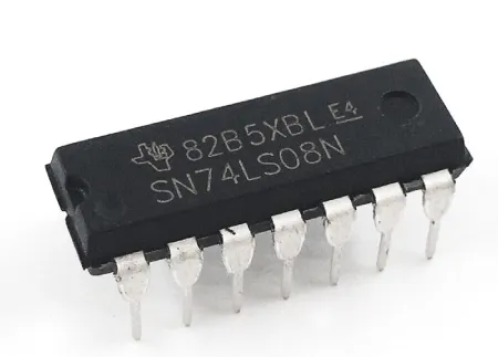
What 74LS08 AND Gate IC is and How It Works
Designing a circuit manually for a single AND gate can be time-consuming due to its complexity. To address this, the 74LS08 AND gate IC is used. There are various logic gate ICs in the same series, including the 74LS00, 74LS73, 74LS02, 74LS138, and 74LS04. This article provides an overview of the 74LS08 AND gate IC and its functionality.
What is the 74LS08 AND Gate IC?
The 74LS08 AND gate IC comprises four independent AND logic gates, allowing each gate to function separately without affecting the others. Hence, it is referred to as QUADRUPLE two-input AND logic gates. This IC operates with a single power supply and is available in multiple packages to suit different circuit requirements.
The series of this IC is the 74XXYY IC series, where the logic gates are designed using Schottky transistors for high-speed logic operations. The output of this IC is always in TTL, allowing it to easily interface with other microcontrollers and TTL devices. The 74LS08 AND gate IC is compact in size and offers high-speed performance, making it reliable for use in various types of devices.
Pin Configuration
The pin configuration of the 74LS08 AND gate IC is illustrated below. This IC features 14 pins, each with its specific functionality, which are detailed below.
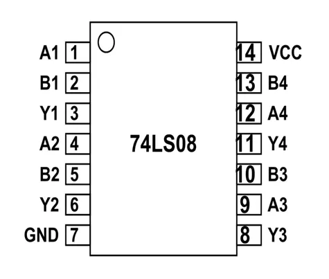
74LS08 AND gate IC
- Pin 1 (A1): This is the first input pin of the 1st AND logic gate within the IC.
- Pin 2 (B1): This is the second input pin for the 1st AND logic gate within the IC.
- Pin 3 (Y1): The first AND gate output can be obtained at this pin.
- Pin 4 (A2): This is the first input pin of the 2nd AND gate within this IC.
- Pin 5 (B2): This pin provides the second input to the 2nd AND gate within this IC.
- Pin 6 (Y2): This pin is used to get the output of the 2nd AND gate from this IC.
- Pin 7 (GND): This is a ground pin; used as a common ground for other communication devices using the IC and power supply.
- Pin 8 (Y3): This pin is used to get the output of the 3rd AND gate from this IC.
- Pin 9 (A3): This pin provides the first input to the 3rd AND gate within the IC.
- Pin 10 (B3): This pin provides the second input to the 3rd AND logic gate within the IC.
- Pin 11 (Y4): This pin is used to get the output of the 4th AND gate from this IC.
- Pin 12 (A4): This pin is the first input of the 4th AND gate.
- Pin 13 (B4): This pin is the second input of the 4th AND gate.
- Pin 14 (VCC): The power supply can be provided to this pin to activate the IC.
Features & Specifications
The specifications and features of the 74LS08 AND gate IC include the following:
- The operating speed of the 74LS08 IC is very fast.
- This IC has low power consumption.
- It features Quadruple 2-Input AND Gates.
- It is available in several packages, including SOP, PDIP, and SOIC.
- It is very simple to operate.
- It is cost-effective.
- The output of this IC is TTL, allowing it to operate with microcontrollers and other devices.
- A single power supply can activate all logic gates within the IC.
- An AND gate can be used independently without affecting other gates.
- The maximum current provided by this IC is 8mA.
- The rise and fall time of this IC is 74LS08.
- The operating voltage of this IC ranges from 4.75V to 5.25V.
- The recommended voltage for this IC is 5V, but it can handle up to a maximum of 7V.
- The operating temperature range is from 0 to 70 degrees Celsius, with a storage temperature range from -65 to 150 degrees Celsius.
How to Use 74LS08 AND Gate IC?
To understand the 74LS08 AND gate IC, one must first recognize how a single AND logic gate works. Generally, an AND logic gate includes three types of combinations, each providing similar outputs for precise inputs.
In the diagram below, we illustrate a transistor-based logic AND gate circuit. This circuit utilizes two transistors acting as switches to determine the output condition based on various inputs. Within the IC 74LS08 AND logic gate, both transistors are connected in series. Power is supplied to the collector terminal of the first transistor, and the output is accessible at the emitter terminal of the subsequent transistor.
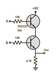
In both transistors, the two inputs are applied to the base terminal. These inputs control the current flow through the transistors. When the input signal is HIGH, current flows through both transistors, resulting in a full voltage output on the output pin.
Alternatively, if one of the input pins is LOW in the circuit, the output will be LOW due to the absence of current flow through the transistors. In this case, the output follows the truth table of an AND gate, as outlined below.
A single AND gate or a combination of two AND gates cannot be used to create any other logic gate. However, an AND logic gate can be transformed into a NAND gate with the addition of a single NOT gate. The AND logic gate is fundamental in the design of other logic gates such as XNOR and XOR, although the creation of these gates requires the use of OR and NOT gates.
Where to Use/Applications of 74LS08 AND Gate IC
The applications of the 74LS08 AND Gate IC include:
- This IC is primarily used to implement general-purpose AND gate logic.
- It finds use in various devices such as servers, ALUs, digital electronics, memory units, and networking devices.
- It is employed in numerous digital systems.
- This IC is essential wherever AND gate logic operations are required, offering 4 AND gates that can be used individually or simultaneously.
- It is particularly valuable in applications requiring high-speed AND gate operations.
- These logic gates are designed with Schottky transistors to minimize switching delays, making them suitable for high-speed AND operations.
- The 74LS08 AND gate IC is cost-effective for AND gate logic operations, widely recognized and readily available.
In summary, the datasheet of the 74LS08 AND Gate IC highlights its provision of 4 AND gates. Compared to manually constructed AND gates, this IC is significantly less expensive. Its compact size and availability in various packages ensure adaptability to small-sized devices. It can interface directly with any TTL device without additional interface devices.
Would you like to know more about the advantages of the 74LS08 logic gate IC?


