


What 74LS138 IC is and How it works
The decoder 74LS138 IC uses advanced technology like silicon (Si) gate TTL technology. These are suitable for different applications like memory address decoding or data routing. These applications feature high-noise resistance and low power utilization typically associated with TTL circuitry. This 74LS138 IC has 3 binary select inputs: A, B, and C. When the IC is activated, these input pins will determine which of the 8 normally HIGH outputs will go LOW. The enable pins include two active low and one active high. The output of the decoder can drive 10 low-power Schottky TTL equivalent loads, and all inputs are protected from static discharge damage with diodes connected to VCC and ground. This article discusses an overview of the 74LS138 IC: 3 to 8 Line Decoder IC.
What is a 74LS138 IC?
The IC 74LS138 is a 3 to 8 line decoder integrated circuit from the 74xx family of transistor-transistor-logic gates. The main function of this IC is to decode or demultiplex applications. The configuration of this IC includes a 3-input to 8-output setup. This IC is primarily used in applications like high-performance memory decoding or data routing. These ICs can minimize system decoding effects in high-performance memory systems. This IC features three enable pins (two active low and one active high), reducing the need for external gates. A 24-line decoder can be implemented without external inverters, while a 32-line decoder requires a single inverter.
This IC is mainly used in demultiplexing applications using an enable pin as a data input pin. Additionally, the inputs of this IC are clamped with Schottky diodes, which are high performance and help contain line ringing and simplify system design.
74LS138 Pin Configuration
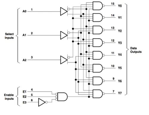
The IC 74LS138 is a 16-pin integrated circuit, and each pin is described below. Similar 74LS138 ICs include:
- Pin 1 (A): Address input pin
- Pin 2 (B): Address input pin
- Pin 3 (C): Address input pin
- Pin 4 (G2A): Active low enable pin
- Pin 5 (G2B): Active low enable pin
- Pin 6 (G1): Active high enable pin
- Pin 7 (Y7): Output pin 7
- Pin 8 (GND): Ground pin
- Pin 9 (Y6): Output pin 6
- Pin 10 (Y5): Output pin 5
- Pin 11 (Y4): Output pin 4
- Pin 12 (Y3): Output pin 3
- Pin 13 (Y2): Output pin 2
- Pin 14 (Y1): Output pin 1
- Pin 15 (Y0): Output pin 0
- Pin 16 (VCC): Power supply pin
74LS138 IC Features
The features of the 74LS138 IC include the following:
- Designed for high-speed operation
- Decoding capability
- Integrates 3-enable pins to simplify cascading
- ESD protection
- Uniform propagation delays
- Supply voltage ranges from 1.0V to 5.5V
- Inputs allow voltages higher than VCC
- Standard propagation delay is 21ns
- Low power consumption: 32mW
- Schottky clamped for high performance
- Operating temperature range: -40ºC to +125ºC
How to Use the 74LS138 IC?
To understand the IC's working, let us design a simple circuit with a few required basic electronic components as shown below. In this circuit, the outputs are connected to light-emitting diodes to illustrate which output pin goes LOW, as the outputs of the IC are inverted.
Here we have used a single device, so the connections of the G2A and G2B pins are connected to GND, followed by linking G1 to VCC to activate the chip.
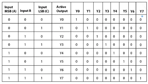
Here, three buttons represent the three input lines for this device. To better understand this concept, refer to the following truth table. In the table, H stands for HIGH, L for LOW, and X for don’t care. The enable pins are G1, G2A, and G2B, where G2 = G2A + G2B.
In the table, the first rows, labeled G1 and G2, are the enable pins that need to be connected correctly; otherwise, all input and output lines will remain high regardless. Once the enable pins are connected, the input lines can be configured to obtain the desired output.
After connecting, if none of the switches are pressed, Y0 will be LOW, and the remaining outputs will be HIGH, as shown in the table above. When B1 is pressed, A0 will be HIGH, and Y1 will become LOW, while the others remain HIGH. When B2 is pressed, A1 will be HIGH, and Y2 will become LOW, while the others remain HIGH. By toggling the three switches, B1, B2, and B3, we can understand the entire truth table, with the inputs being A0, A1, and A2.
Applications of 74LS138 IC
The applications of IC 74LS138 include:
- - Line decoders
- - Memory circuits
- - Servers
- - Digital systems
- - Line demultiplexing
- - Telecom circuits
Thus, this covers the data sheet of the 3 to 8 line decoder 74LS138 IC. As discussed previously, this IC is specifically designed for use in high-performance memory decoding and data routing applications requiring minimal propagation delay times. The data transfer rate of a memory unit determines the performance of any application, and delays of any kind are not acceptable. Therefore, the IC 74LS138 line decoder is ideal for such applications. The holdup times of this IC are less than the typical memory access time, meaning the minimal system delay introduced by the decoder has negligible effect on performance.
Related Articles
What is BT136 600E TRIAC? Pinout and Applications
LM358 IC:Features,Applications and Types
What is Analog to Digital Converter & How it works


