


What is Amorphous Silicon Solar Cell?
The thin-film cells featuring amorphous silicon are an alternative to traditional solar cells. Producers have crafted these cells utilizing top-notch amorphous silicon material.Functioning as semiconductors, these cells are integrated into thin films composed of various materials such as metal, glass, and plastic.A commercially available amorphous silicon solar cell possesses a notable absorption capacity, making it well-suited for low-power devices like pocket calculators.Furthermore, this specific solar cell exhibits superior efficiency compared to both monocrystalline and polycrystalline cells.
What is Amorphous Silicon Solar Cell ?
Currently, silicon stands as the dominant material in the photovoltaic sector for crafting solar cells, with three primary variants: monocrystalline silicon solar cells, polycrystalline silicon solar cells, and amorphous silicon solar cells. The first two necessitate a specific thickness for effective solar energy absorption, given their status as indirect bandgap semiconductors. Due to the substantial thickness of the PN junction (often exceeding 200 microns), more silicon raw material is required, leading to increased costs. The expense associated with solar panels remains significant, compounded by the considerable silicon waste generated. Silicon, a pivotal and highly adaptable semiconductor, is central to this scenario.
Contrastingly, amorphous silicon boasts broad-spectrum light radiation absorption, requiring a minimal thickness, and functions as a direct bandgap semiconductor. Consequently, thin film solar cells made from amorphous silicon can be remarkably thin. The market favors amorphous silicon due to its cost-effectiveness and superior performance, with the entire thickness of the light absorption sheet approximating 1 micron.
Features of amorphous silicon solar cells
Cost-effectiveness
Achieving complete light absorption with minimal material usage is feasible through silicon, particularly with amorphous silicon requiring a mere one-micron thickness compared to the 200 microns for single crystals (attributed to amorphous silicon's substantial light absorption coefficient).
Silane, the principal raw material for high-purity polysilicon manufacturing, is readily available in large volumes from the chemical industry at a low cost (6% cost efficiency).
The thickness disparity of 240 to 270 um in crystalline silicon solar cells highlights the need for numerous semiconductor grades in large-scale production. Silicon wafers alone constitute 65-70% of the total solar cell cost, with the material cost exceeding RMB22 per watt in China. Amorphous silicon solar cells and other thin-film counterparts emerge as the sole feasible options for electricity generation on a significant scale due to raw material supply considerations.
Ease of Large-Scale Formation
Modification of gas phase composition or flow facilitates the production of pn junctions and laminated structures, enabling full automation. The core method suits the creation of fault-free a-Si alloy thin films over expansive areas.
Variety and Flexibility
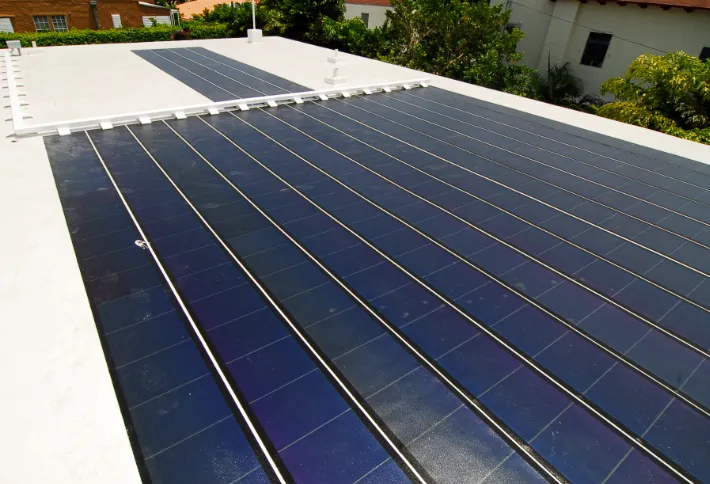
Integration of thin-film a-Si solar cells is straightforward, allowing for arbitrary development of device power, output voltage, and output current. This versatility facilitates the creation of diverse products for various applications, including low-power sources for indoor use (e.g., watch and calculator batteries). The silicon mesh structure's excellent mechanical qualities make a-Si film ideal for flexible substrate-based light solar cells. Adaptable manufacturing techniques enable the creation of building-integrated batteries, making them suitable for rooftop solar power systems in homes.
Amorphous silicon circumvents lattice mismatch issues, allowing easy application over vast areas on virtually any substrate, including cost-effective glass substrates.
Optimal Performance
Amorphous silicon thin-film cells outperform single-crystalline silicon cells by generating 15% more power annually under identical lighting conditions. The efficiency-to-mass ratio is also superior, making amorphous silicon six times more efficient than monocrystalline cells, positioning it favorably for future space solar power plant construction.
Evolution of Amorphous Silicon Solar Cells
Since 1974, researchers delved into the study of amorphous silicon solar cells, recognizing the potential of doped amorphous silicon thin films in solar applications.
During this initial phase, the conversion efficiency was below 1%, as reported by Carlson from RCA, who pioneered amorphous silicon solar cells employing metal-semiconductor and p-i-n device architectures.
In 1977, Carlson achieved a significant advancement, elevating the conversion efficiency of amorphous silicon solar cells to 5.5%.
The integration of amorphous silicon solar cells into practical applications began in 1978, marked by their use in Japan.
In 1980, employing a metal-insulator-semiconductor (MIS) structure, ECD successfully created amorphous silicon solar cells with a notable conversion efficiency of 6.3%. This innovation extended to the integration of silicon solar cells into pocket calculators.
The year 1982 witnessed a broader incorporation of amorphous silicon solar cells into various consumer goods, including watches, chargers, radios, and more.
From 1984 onward, composite solar cells utilizing amorphous silicon found utility as standalone power sources.
The ascendancy of amorphous silicon solar cells continued, establishing them as the most promising type in the solar cell domain. Consequently, their standing within the semiconductor solar cell industry improved significantly. Presently, amorphous silicon solar cells dominate civilian applications and contribute approximately one-third to the global solar cell production in terms of electric power.
Structure of Amorphous Silicon Solar Cells
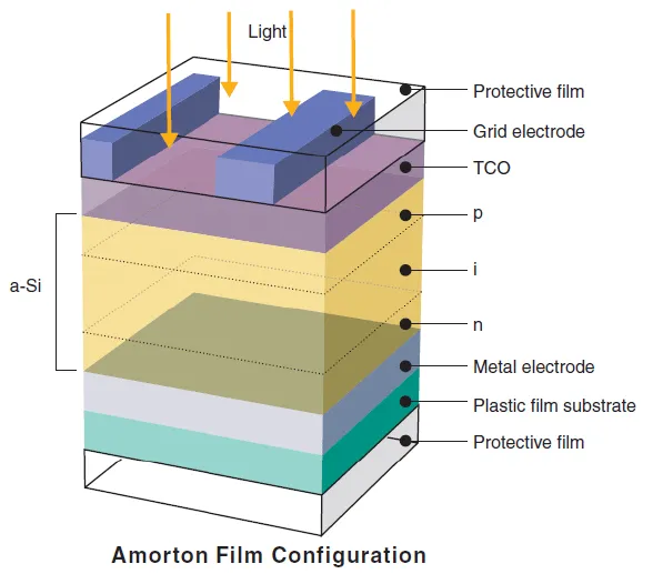
Unlike monocrystalline silicon solar cells, commonly featuring a p-n structure, amorphous silicon solar cells typically adopt a p-i-n structure. This choice is influenced by the smaller Fermi level shift in lightly doped amorphous silicon, resulting in reduced band bending when employing substantially doped materials on one side and lightly doped materials on the other. The direct formation of a p+-n+ junction using heavily doped p+ and n+ materials leads to a lower minority carrier lifetime due to the heightened density of defect states in heavily doped amorphous silicon, thereby diminishing battery performance. Consequently, an undoped amorphous silicon layer is often deposited between the two substantially doped layers to form the active collector area.
In contrast to crystalline silicon solar cells, where photogenerated carriers primarily diffuse, amorphous silicon solar cells rely on carriers generated in the undoped i-layer. The electric field within the solar cell facilitates the drift motion of these photogenerated carriers.
The thin and nearly transparent top layer in amorphous silicon solar cells, heavily doped, permits incident light to pass through to the undoped layer, generating free photogenerated electrons and holes. The built-in electric field extends from this point, swiftly sweeping photogenerated carriers to the n+ and p+ sides upon production.
Undoped amorphous silicon, being inherently a weak n-type material, can be converted into an i-type by centering the Fermi level with a trace amount of boron during the deposition of the active collector region, enhancing solar energy efficiency. To naturally dope the active collector region with boron when forming the p-layer, the deposition sequence is often set as p-i-n during the preparation process. Following this deposition sequence, the transparent conductive substrate cell consistently faces the p+ layer, while the opaque substrate cell faces the n+ layer.
Tandem amorphous silicon cells aim to maximize solar energy efficiency across a broader range of wavelengths. Given the broad energy distribution of the solar spectrum, single-junction solar cells, even when made of crystalline materials, face a theoretical maximum conversion efficiency of around 25% under AM1.5 light. To address this limitation, solar spectrum divisions guide material selection with matching energy gaps. This construction, illustrated in the figure, results in laminated solar cells.
Production and Manufacturing Process of Amorphous Silicon Thin Film Solar Cells
Key equipment used in the production of amorphous silicon thin film solar cells includes conductive glass cleaning and edging equipment, large-scale amorphous silicon thin film PECVD production equipment, infrared and green laser engraving equipment, large magnetron sputtering production equipment, and component testing equipment.
Grinding: Chamfer the eight edges of the clear conductive glass, removing any sharp corners.
Once-off cleaning: Thoroughly wash and dry the transparent conductive glass surface on both sides.
Laser Engraving: Prevent sub-battery short-circuiting by laser-engraving lines on the conductive glass, ensuring a specific resistance (> 1M ohm, typically 20K in production).
Secondary Cleaning: Wash, dry, and ensure the conductive glass surface is spotless.
Loading: Insert the conductive glass into the workpiece frame for heating and coating, ensuring the conductive glass film surface doesn't reverse during loading.
Preheating: Heat the conductive glass evenly to the temperature required for PECVD deposition (215°C in the preheating furnace).
PECVD: Apply a large-area uniform PIN layer to the conductive glass under vacuum conditions, ensuring no chromatic aberration or stripes on the battery chip after deposition.
Cooling (Unloading): After cooling in the workpiece rack, unload the glass cautiously to prevent flexing or breakage.
Green Laser Scribing: Use a 532nm green laser to scribe lines on the partially finished chip, creating a conductive channel for sub-battery attachment.
PVD (Magnetron Sputtering): Plate the back electrode (AL or AZO+AL), ensuring the battery chip does not peel after aluminum plating, and the back electrode resistance is less than 10 ohms.
Three Laser Scribing: Scribe lines on the partially finished chip with an aluminized back electrode to complete the series connection of sub-cells.
Sweep the Edge: Clear a 10mm area along the chip's four edges to achieve insulation.
Annealing: Heat-treat the thin film material's microstructure to enhance stability and increase the battery chip's conversion efficiency.
Check: Verify the battery chip's electrical specifications.
Back-Pressure: Fix flaws in the chip to enhance conversion efficiency.
The production process for amorphous silicon thin film solar cells is notably swift compared to other photovoltaic cells. However, from film design to process control, the vacuum PECVD fabrication requirements for amorphous silicon semiconductor films are stringent.
While large-area modules have not yet reached the authorized efficiency of 6% on most manufacturing lines, laboratory-prepared small-area cells boast approximately 15% photoelectric conversion efficiency. The variation in conversion efficiency between small and large-area components indicates a production line's technical sophistication. Some amorphous silicon production lines have achieved modules with certified efficiency over 8%, showcasing superb performance under actual operating conditions.
Amorphous silicon photovoltaic modules offer unique advantages, including low manufacturing costs, moderate photoelectric conversion efficiency, beautiful translucent modules, bendable and unbreakable flexible components. Despite challenges from other types of photovoltaic modules, amorphous silicon remains indispensable for power generation applications due to its superior performance in real-world conditions.
Deficiencies in Amorphous Silicon Materials - Photodegradation Phenomenon
The photodegradation effect poses a significant challenge for hydrogen-doped amorphous silicon thin films employed in solar cells. This issue arises due to the vulnerability of the Si-H bond (with a bond energy of 323). When hydrogenated amorphous silicon films are subjected to intense light or prolonged current exposure, the weak Si-H bond rapidly loses hydrogen, leading to the generation of a substantial number of Si dangling bonds. This, in turn, diminishes the electrical characteristics of the film. The loss of hydrogen initiates a cascade effect, with the dangling bond attracting neighboring hydrogen atoms. This loosening of the Si-H bond prompts adjacent hydrogen atoms to combine into H2 (H-H bond energy of 436), facilitating the formation of H2 bubbles. The prolonged exposure to light results in a notable decline in the photoelectric conversion efficiency of solar cells.
Amorphous silicon solar cells encounter limitations in conversion efficiency due to the material's insensitivity to the long-wavelength segment of the solar radiation spectrum, attributed to its optical band gap of 1.7 eV.
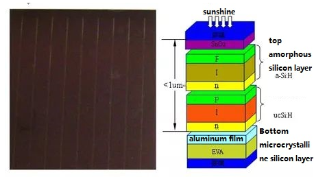
To counteract the diminished light absorption caused by thinning thickness and mitigate the photodegradation impact, a multi-level solar cell group can be devised by connecting numerous batteries in series. This approach allows for a reduction in the thickness of the i-layer within the battery, enhancing light absorption. Tandem solar cells replicate one or more p-i-n single junction solar cells on their constructed counterparts.
Layering one PIN junction upon another, as illustrated in the diagram above, characterizes tandem amorphous silicon solar cells. The fundamental concept driving these cells is rooted in the understanding that any semiconductor material can only absorb photons whose energy surpasses its energy gap value, given the broad energy distribution in the solar spectrum. Photons with lower energy levels from sunlight traverse through the battery, get absorbed by the metal in the back electrode, and are converted into heat energy. Conversely, high-energy photons with energies exceeding the energy gap width transfer their energy to the battery material through the pyrolysis of photogenerated carriers, causing the material's lattice structure to heat up. Unfortunately, these energy forms cannot be efficiently converted into electrical energy usable by photogenerated carriers for delivery to a load. Consequently, the theoretical maximum conversion efficiency for single-junction solar cells often hovers around 25%, even when comprised of crystalline materials.
To optimize light energy conversion into electrical energy, the solar spectrum can be dissected into distinct parts, with each battery constructed from a material possessing the best energy band width match for that specific part. These batteries are then superimposed from the outermost to the innermost layer based on the energy gap, ranging from the largest to the smallest. The outermost wide-gap material cell utilizes the light, while longer-wavelength light can penetrate and be harnessed by the narrower energy-gap material cell. Laminated cells exemplify one type of cell structure embodying this approach.
The efficiency of amorphous silicon cells, impacted by reduced conversion efficiency due to photo-induced degradation wherein the H-H bond is broken and the Si-H bond is re-formed, can be restored to 80%-97% of the original value through annealing at 130-175 degrees Celsius—an restorative capability not present in other batteries.
Factors Influencing Amorphous Silicon Cell Performance and Prospects for Development
The extensive disordered random network structure inherent in amorphous silicon significantly scatters carriers, impeding their efficient collection. Unlike monocrystalline silicon solar cells, the p-n structure is generally not employed in amorphous silicon solar cells to enhance conversion efficiency and stability. This decision stems from the fact that lightly doped amorphous silicon exhibits a minute Fermi level shift, leading to reduced energy band bending and alterations in the battery's open circuit voltage when both sides are lightly doped or when one side is weakly doped and the other strongly doped. To address this limitation and counter the negative impact of severely doped amorphous silicon material, which results in a high density of defect states and short minority carrier lifetime, the creation of a p-i-n structure involves placing an undoped amorphous silicon layer (i-layer) between two strongly doped layers.
In contrast to crystalline silicon solar cells, where carriers primarily migrate through diffusion, photogenerated carriers are predominantly generated in the undoped i-layer of amorphous silicon solar cells. The small drift movement of carriers is primarily driven by the battery's electric field. Despite the ability of an amorphous silicon battery with a pin structure to operate in the presence of light, the impact of light-induced deterioration introduces instability, leading to a gradual decline in conversion efficiency over time. Consequently, further optimization of the battery's structure and manufacturing process is necessary.
The key variables influencing the conversion efficiency and stability of amorphous silicon cells include the characteristics of the transparent conductive film, window layer properties (such as optical band gap width, conductivity, and doping concentration), window layer activation energy, window layer light transmittance, energy gap matching, interface state (density of interface defect state), thickness of each layer (especially the I layer), and solar cell design, among other factors. Amorphous silicon thin-film cells typically feature integrated heterojunctions.
Amorphous silicon cells, produced through an energy-efficient and low-heat technique, are gaining market share annually. Currently, over half of thin-film solar cell companies utilize amorphous silicon thin-film technology, and it is expected that amorphous silicon thin-film will hold a substantial share in future thin-film solar cells in the coming years. However, challenges such as low photoelectric conversion efficiency and light-induced deterioration persist. To overcome these challenges and enhance efficiency and stability, exploration of novel device structures, materials, processes, and technologies is imperative.
For example, stacked and integrated battery structures are employed, and in the realm of transparent conductive films, the use of films with low resistivity, ion pollution blocking capability, increased incident light absorption, and anti-radiation properties is explored. In the area of window layer materials, research is conducted on new materials with wide optical band gaps and low resistance, such as amorphous silicon carbon and amorphous silicon oxygen. Enhancement of amorphous silicon film preparation techniques, such as RF-PECVD, ultra-high vacuum PECVD, very high frequency (VHF) PECVD, and microwave PECVD, is pursued to improve carrier transport capability, electron density, and photon life of the film. Interface treatment involves the use of buffer layer insertion and hydrogen passivation technology to reduce interface recombination loss and enhance battery short-circuit current and open-circuit voltage. While challenges persist, numerous solutions to improve amorphous silicon thin film cells are conceivable, and widespread use of thin-film solar cells is anticipated.


