


PT2399 Digital Delay IC: Pinout, Specs & Circuit Guide
What Is the PT2399 Digital Delay IC?
The PT2399 is a digital audio delay processor IC, based on CMOS, designed to be used in the echo and delay applications. It combines all the primary signal processing units needed to do digital delay, such as input buffering, ADC conversion, dynamic RAM storage, digital clock control, output filtering and DAC reconstruction. By adjusting a single external resistor, designers can vary the internal sampling clock, which directly controls the delay time.
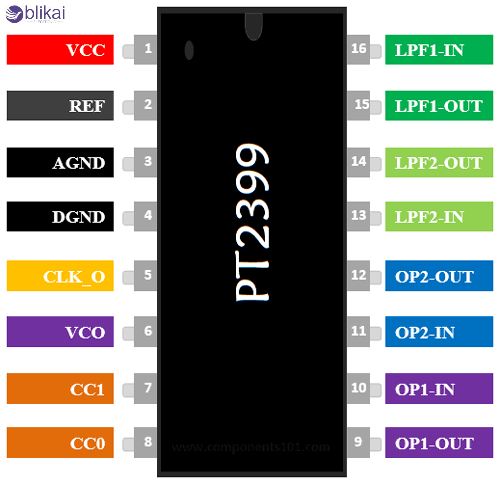
PT2399 Pinout Diagram and Pin Functions
The PT2399 has more often than not been offered in DIP-16 and SOP-16 formats, which makes it applicable to both breadboard-based prototyping and tiny PCB layouts. The pins have a certain purpose concerning audio input, audio output, clock generation, filtering, and power management.
PT2399 Pin Configuration Table
|
Pin |
Name |
Function Description |
|
1 |
VCO |
External resistor connection for clock control |
|
2 |
LPF1 |
Low-pass filter connection |
|
3 |
LPF2 |
Low-pass filter connection |
|
4 |
AGND |
Analog ground |
|
5 |
REF |
Internal reference voltage output |
|
6 |
OP1 |
Output amplifier 1 |
|
7 |
OP2 |
Output amplifier 2 |
|
8 |
VSS |
Ground |
|
9 |
VDD |
+5 V power supply |
|
10 |
LPF3 |
Low-pass filter input |
|
11 |
LPF4 |
Low-pass filter output |
|
12 |
OP_IN |
Operational amplifier input |
|
13 |
OP_OUT |
Operational amplifier output |
|
14 |
IN |
Audio signal input |
|
15 |
NC |
Not connected |
|
16 |
NC |
Not connected |
Detailed Pin Function Explanation
The most important pin in the PT2399 design is the VCO pin because it has a direct relationship with the internal clock frequency and hence the delay time. By connecting a resistor between this pin and ground, designers can precisely adjust the delay. The internal low-pass filtering network is made of LPF pins, which minimize noise and clock artifacts in the high frequency range. The REF pin provides a stable bias reference voltage, typically around half the supply voltage, which ensures proper signal centering. The Operations of OP1 and OP2 give amplified output signals, making them interfaceable to mixers or amplifiers.
Absolute Maximum Ratings and Electrical Specifications
Absolute Maximum Ratings
|
Parameter |
Rating |
|
Supply Voltage |
6.5 V |
|
Input Voltage |
-0.3 V to VDD + 0.3 V |
|
Storage Temperature |
-40°C to +125°C |
|
Operating Temperature |
-20°C to +85°C |
Recommended Operating Conditions
|
Parameter |
Typical Value |
|
Supply Voltage |
5.0 V |
|
Operating Temperature |
0°C to +70°C |
|
Clock Frequency |
2 kHz – 40 kHz |
Key Electrical Characteristics
There is a delay time which can be regulated between 30 ms and 340 ms by the PT2399. The signal-to-noise ratio is usually more than 85 dB, and the total harmonic distortion is kept to less than 0.5% under normal working conditions. Current consumption is typically below 30 mA, making it ideal for battery-powered effects pedals and portable audio modules.
Internal Block Diagram and Working Principle
On the inside, the PT2399 takes the analog audio signals it receives and changes them into digital form with an internal ADC. These digital samples get stored in dynamic RAM under the action of an internal clock generator. A programmable delay is then applied to get the stored samples and then reconstructed back into analog form using an internal DAC. An array of low-pass filters filters the output waveform to reduce noise and aliasing in digital. The delay time is directly proportional to the sampling rate, which in turn is directly proportional to the clock frequency, by modifying the clock frequency using an external resistor, thus directly modifying both the delay time and audio bandwidth.
How the PT2399 Delay Control Works
The delay time of the PT2399 is determined by the internal clock frequency, which is set through a resistor to the VCO pin. The smaller the values of the resistor, the higher the clock frequency, which leads to a reduction in delays and a higher audio bandwidth. Increasing the value of resistors decreases the clock frequency, creating more delays, but also decreases bandwidth and increases noise.
Typical Application Circuits of PT2399
Basic Digital Delay Circuit
A simple PT2399 delay circuit demands a small fraction of external components, such as a clock-setting resistor, coupling capacitors and low-pass filter components. This simple configuration provides a clean echo suitable for basic audio enhancement.
Guitar Delay Pedal Circuit
The PT2399 is usually combined with operational amplifiers to do input buffering and mixing of the output in guitar pedals. A feedback loop is often added to create multiple repeats, enabling rich and atmospheric delay effects.
Karaoke Echo Effect Circuit
The Karaoke systems often incorporate PT2399 circuits to increase the depth and quality of voice. Feedback and delay adjustment have enabled the users to make the echo sensitivity suitable for the various singing styles.
Audio Mixer Echo Module
Compact audio mixers also use PT2399 modules to incorporate built-in echo effects without external processors, which makes the system design more basic and less expensive.
PT2399 Reference Circuit Diagram Explanation
A standard PT2399 reference circuit includes power supply decoupling capacitors, a clock resistor, biasing networks, coupling capacitors, and output filters. The input audio is biased around the REF voltage, ensuring symmetrical signal swing. The output stage includes low-pass filtering to suppress clock noise and digital artifacts, resulting in smooth and natural-sounding delay.
Selecting External Components for PT2399 Circuits
In order to produce optimum performance, precision resistors of low temperature coefficients must be employed in clock control by the designer. Signal coupling and filtering, and low-noise operational amplifiers such as NE5532 or TL072 are suggested to be used with ceramic or film capacitors. Proper PCB grounding and short signal paths are essential to minimize noise.
PT2399 Delay Time Calculation and Design Formula
The delay time (T) can be approximated in the formula as the approximate delay time (T):
T ≈ (R × 0.03)
where R is the external resistor value in kilo-ohms, indicatively, a 50 kO resistor will represent a delay of about 150 ms. By using fixed resistors in conjunction with potentiometers, designers can be able to fine-tune performance when dealing with delay.
Audio Performance Optimization Techniques
Multi-stage low-pass filtering, star grounding, and appropriate shielding should be used to reduce digital noise and clock interference by the designers. Both ceramic and electrolytic capacitors are decoupled and are used to guarantee a stable power supply. Location of high-frequency clock traces off important analog paths also enhances the audio quality.
Common Problems and Troubleshooting Guide
No Output Sound
Common causes include incorrect biasing, faulty coupling capacitors, and wiring errors. Verifying power supply voltage and reference bias is essential.
Excessive Noise and Whine
Clock noise coupling and poor grounding are the primary culprits. Improving filtering and PCB layout typically resolves these issues.
Distorted or Clipped Output
Excessive input signal amplitude or improper gain staging can cause distortion. Reducing the input level and optimizing the amplifier gain solves the problem.
PT2399 vs Other Audio Delay ICs
The PT2399, in comparison to traditional bucket-brigade delay chip designs, including the MN3005, has a simple circuit design, reduced cost and improved stability. DSP-based delay processors have better audio quality and programmability, but need a more complicated firmware, and are more expensive to develop, which makes PT2399 a viable tradeoff in many applications.
Typical Applications of the PT2399
The PT2399 is widely used in guitar pedals, vocal processors, DJ mixers, sound effect modules, toys, intercom systems, and consumer audio electronics. This has allowed it to remain a popular choice by both amateur and professional designs due to its versatility and ease.
Advantages of PT2399
Low cost, simple design, integrated ADC/DAC, compact form factor, and wide community support.
Disadvantages of PT2399
Poor bandwidth at long delay times, digital noise and a non-programmable nature when compared to contemporary DSP offerings.
FAQs
How do I reduce digital noise in PT2399 circuits?
Digital noise can be reduced through better power supply decoupling, grounding layout, low-pass filtering and separation of PCB traces. External audio connection is also much improved by using a shielded cable and grounding the enclosures.
Can PT2399 work with Arduino or microcontrollers?
The PT2399 can be easily fitted to Arduino and audio projects based on microcontrollers. Although it does not offer digital control interfaces, microcontrollers may be used to control analog control voltages with digital potentiometers or with DAC output to dynamically control delay.
Is PT2399 suitable for professional audio equipment?
The PT2399 is mainly intended for consumer and semi-professional audio products. Although it has a great price-to-performance ratio, high-quality studio-level equipment will usually need faster sampling rates, increased bandwidth, and reduced noise floors that are only possible with newer DSP processors.
Conclusion
One of the most feasible and popular ways to achieve digital effects of echo and delays is still the PT2399 Digital Delay IC. Its combined design, low external components, and adjustable delay made it an ideal application in guitar effect pedals, karaoke systems, DJ mixers, and other DIY audio applications.
Some images are sourced online. Please contact us for removal if any copyright concerns arise.


