


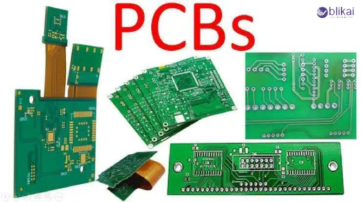
What Is a PCB? Printed Circuit Board Basics & Applications
Introduction to Printed Circuit Boards (PCBs)
Most of the electronics of the present day are based on PCBs or printed circuit boards. They offer a dependable base on which to mount, interconnect and enclose electronic parts so that they can perform reliably in small size designs. PCBs are required in the circuit integrity, noise reduction, and thermal management of simple consumer products through to complex industrial systems.
What Is a PCB? (Printed Circuit Board Explained)
A PCB comprises a flat board of insulating material onto which conductive pathways are etched, printed or laid down on the surface. These conductive traces substitute conventional wiring, forming systematic electrical connections among elements and making automated production. PCBs reduce signal interference by mechanical support of components and electrical connection through reliable layout, enhance assembly error reduction, and are also capable of making precise and repeatable designs. They form the core of gadgets down to microcontrollers as well as industrial machines.
Main Components of a PCB
Substrate Material
The base material of a PCB is known as the substrate, and this material gives the PCB its mechanical strength, electrical insulation, and thermal stability. The most used substrate is FR-4 fiberglass because it has a tradeoff of durability, heat resistance, and affordability. Flexible PCBs use polyimide or polyester substrates, allowing boards to bend or fold without breaking, which is crucial for wearable electronics, foldable devices, and compact assemblies.
Copper Layers and Traces
Copper layers form the conductive paths that carry electrical signals and power across a PCB. The design of these traces affects signal quality, current capacity, and impedance. High-speed circuits require precise trace width and spacing, while multilayer PCBs can include dedicated power and ground planes to reduce noise and improve performance. Copper thickness and layout directly impact both the electrical and thermal characteristics of the board.
Solder Mask and Silkscreen
The solder mask is a protective coating applied over copper traces to prevent oxidation, short circuits, and solder bridging. It also improves mechanical strength and environmental resistance. The silkscreen layer provides printed labels, symbols, and component references, assisting assembly, testing, and maintenance. The combination of these layers increases reliability, lowers the manufacturing errors, and makes the board look good.
Electronic Components on a PCB
PCBs host a wide range of electronic components, including resistors, capacitors, diodes, transistors, integrated circuits (ICs), and connectors. Components are mounted using surface-mount technology (SMT) or through-hole techniques, depending on mechanical and thermal requirements. Effective traces design and appropriate location and positioning of the components result in an effective, reliable, and safe functioning of the device.
Types of Printed Circuit Boards
Single-Sided PCBs
Single-sided PCBs have conductive traces on one side of the board. They are cheap and easy, which are used in low density circuits, toys, domestic appliances and simple electronics whereby complex routing is not required.
Double-Sided PCBs
The PCBs are double sided with copper on both sides thus they have more density in components and complex circuits. Traces between layers are connected by vias, which make them suitable for industrial devices, automotive electronics and relatively complex consumer goods.
Multilayer PCBs
Multilayer PCBs contain three or more conductive layers laminated together. This type of construction enables very high component density, improved signal quality and advanced power distribution. Multilayer PCBs are also being used in computers, servers, communication equipment, and aerospace electronics.
Flexible and Rigid-Flex PCBs
Flexible PCBs are able to bend, fold and twist, which offer flexibility to the design in tight spaces. Rigid-flex PCBs combine rigid sections with flexible parts, reducing the need for connectors and cables, improving reliability, and enabling compact designs in medical devices, drones, and wearable electronics.
High-Frequency and HDI PCBs
High-frequency PCBs are optimized for fast signal transmission, minimizing signal loss and reflection. The High-Density Interconnect (HDI) PCBs can use tiny components and fine traces, which is why they should be used with smartphones, 5G communication devices, and high-performance computers.
How Does a PCB Work?
PCBs operate based on the circuit design by guiding electrical signals and power over copper traces, vias and pads which link electronic components together. Power layers and ground planes assist in the control of noise, crosstalk as well as voltage stability. Appropriate layout and trace design ensures signal integrity, low electromagnetic interference and efficient operation of devices even in the state of high computation load.
PCB Manufacturing Process (Overview)
The computer-aided design (CAD) and layout are the starting steps in the PCB manufacturing process which is then followed by etching copper layers and to add additional layers which may or may not be necessary. Connection between layers is formed by drilling and plating, and a solder mask and silkscreen protect and label. Lastly, parts are put into place and soldered using automated assembly machines. The quality control, testing, and inspection are used to ensure that every PCB is of performance and reliability before it is deployed in the field.
Common PCB Applications
Consumer Electronics
Smartphones, laptops, televisions and home-based appliances use PCBs to provide compact and light designs with high reliability. They facilitate all the activities of power management and signal processing that can improve functionality of common devices.
Industrial and Automation Equipment
In factories and industrial settings, PCBs control machinery, sensors, and automated systems. They must be able to withstand such extreme environments as temperatures, vibration and electrical noise without compromising on their accuracy.
Automotive Electronics
The use of PCBs in modern vehicles is in the engine control unit, infotainment, safety, lighting, and electric vehicle power management. PCBs enhance efficiency, reliability and safety and allow innovative capabilities such as autonomous driving.
Medical Devices
PCBs are used in medical electronics in diagnostic equipment, monitoring equipment and life-support equipment. The reliability, the small size and the accuracy of performance are all essential in providing patient safety and accurate outcomes.
Communication and IoT Devices
All the routers, gateways, smart sensors, and IoT devices rely on PCBs as sources of wireless communication, data processing, and network connectivity. PCBs facilitate miniature and energy-saving as well as very dependable devices that are mandatory in contemporary interconnected systems.
Advantages of Using PCBs
PCBs are small in design, have predictable electrical behaviour, are reliable, and have fewer errors in assembly. They ease the production process, facilitate fast signals, reduce noise, and enable the production to be scaled. With PCBs, cost reduction, durability and stability of the electronic systems over time has also been improved.
PCB vs Other Circuit Assembly Methods
Compared to point-to-point wiring, PCBs provide cleaner layouts, higher reliability, and easier troubleshooting. Breadboards are utilized in prototype applications, whereas PCBs are done with permanent and production-ready applications. This has seen PCBs being the preferred choice of consumer and industrial electronics.
Key Factors to Consider When Choosing a PCB
Choosing the right PCB involves considering substrate material, layer count, operating environment, thermal and mechanical stresses, electrical performance, and cost. Optimal performance, life and efficiency are guaranteed with proper selection particularly in the high-density or high-speed applications.
Future Trends in PCB Technology
The PCB technology is driving miniaturization, increasing the number of layers, flexibility, and new materials. Artificial intelligence, electric cars, wearables, and the 5G network are among the newest fields that are transforming the design, production, and functionality of electronics and making up the future of electronic devices.
FAQ
Can PCBs be repaired?
Minor faults like broken traces or solder issues can sometimes be repaired, but complex damage usually requires board replacement.
Are PCBs recyclable?
PCBs are recyclable by using special procedures that extract metals and minimize environmental footprint although recycling is not as simple as that of common plastics or metals.
Conclusion
The cornerstone of modern electronics are PCBs which allow compact, reliable, and scalable designs to the industries. Today, it is essential to know the basics, types, and uses of PCBs to work in the sphere of consumer gadgets, industrial devices, or even medical equipment, and be a professional engineer, designer, or electronics enthusiast. With the development of technologies, PCBs also develop, facilitating the invention of AI, IoT, wearables, and fast communication.
Some images are sourced online. Please contact us for removal if any copyright concerns arise.


