


What Is a PCB Board? Full Technical Explanation
What Is a PCB Board?
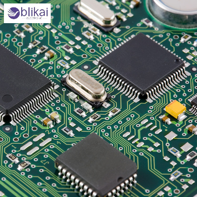
A Printed Circuit Board (PCB) is a flat board composed of insulating substrate material laminated with copper conductive layers, which create electrical circuits to connect electronic components. These are conductive tracks, which are also called traces, that are used instead of the old wiring and enable signals and power to pass effectively between components on the board.
Basic Structure of a PCB Board
Core Layers of a Typical PCB
A common PCB board comprises four main layers, namely substrate, copper layers, solder mask and silkscreen. The substrate has typically become the fiberglass-reinforced epoxy (FR-4), which has been made into a mechanical base. Copper layers are used to offer electrical conductivity, and the solder mask is used to prevent copper traces from being oxidized and causing unintentional shorts. The silkscreen layer has reference marks, component labels and orientation marks.
Layer Stack-Up Explained
PCBs can be single, double-layered or multi-layered. Single-layer PCBs have copper on one face, twice-layered PCBs have copper on both sides, and multilayer PCBs consist of layers of copper that are interspersed with insulating materials. Multilayer designs allow high circuit density, reduced electromagnetic interference, and enhanced power distribution.
PCB Materials Explained – Substrates, Copper & Coatings
Common PCB Substrate Materials
FR-4 is the most common substrate used as it has great mechanical strength, flame resistant, electrical insulation and is cost-effective. Aluminum-based substrates are employed in high-power and LED applications for superior thermal conductivity. Polyimide materials are used in flexible PCBs for dynamic bending applications, while high-frequency materials such as Rogers laminates offer low dielectric loss for RF circuits.
Copper Foil Types and Thickness Standards
Copper thickness is usually expressed in ounces per square feet with the standard in the industry being 1 oz (35 um). Thicker copper layers, such as 2 oz or 3 oz, are used in power electronics to handle higher currents. Copper foils are very crucial in PCBs that have high frequencies to ensure that signal losses are minimized by the use of smooth copper foils.
Solder Mask and Surface Finishes
Surface finishes protect exposed copper pads and ensure reliable solder joints. Common finishes include Hot Air Solder Leveling (HASL), Electroless Nickel Immersion Gold (ENIG), Organic Solderability Preservatives (OSP), and immersion silver. Both of them possess their individual advantages in terms of solderability, durability and cost.
Types of PCB Boards and Their Applications
Single-Sided PCBs
Single-sided boards contain components on one side only and are widely used in simple, low-cost electronics such as calculators, power supplies, and LED lighting modules.
Double-Sided PCBs
Double-sided PCBs allow component mounting and copper routing on both sides, enabling higher circuit density and improved performance in consumer electronics and industrial controllers.
Multilayer PCBs
Multilayer PCBs use three or more conductors and are necessary for complicated devices like smartphones, computers, network equipment, and embedded systems.
Flexible PCBs (FPC)
Flexible circuits are designed on the substrate of polyimides that are very fine and therefore can be bent, folded and twisted. Wearable electronics, cameras and medical appliances are the typical applications of these.
Rigid-Flex PCBs
Rigid-flex boards integrate rigid and flexible dies into one single IC, which has the benefits of high reliability and space-saving in aerospace and military systems.
HDI PCBs
High-Density Interconnect PCBs are designed with tiny holes, narrow tracks and sophisticated stacking processes to produce very miniature designs, in which they serve smartphones and sophisticated digital systems.
How Does a PCB Work? – Electrical and Mechanical Principles
Signal Flow and Current Path Explanation
The circuits use copper traces through which electrical signals are transmitted that connect components in the circuit schematic. The networks of power distribution give constant voltages, and ground planes give reference potential and noise suppression.
Role of Traces, Vias, Pads, and Planes
The traces are conductors, the vias are adopted to connect the layers to each other, the pads provide a soldering point where the components can be soldered, and the planes are adopted to offer even power and grounds to the whole board.
Impedance, Crosstalk, and EMI Considerations
The recent PCB design is very keen on trace impedance, spacing and routing geometry so that signal distortion, crosstalk, and electromagnetic interference are minimized to achieve reliable high-speed data transmission.
Key PCB Components and Layout Elements
Traces, Pads, and Vias
Traces form conductive pathways, pads anchor components, and vias enable vertical electrical connections between layers, forming the foundation of multilayer circuit routing.
Power Planes and Ground Planes
Special planes enhance voltage stability and decrease noise and increase thermal dissipation, and are therefore essential in high-speed and high-current uses.
Fiducials and Mechanical Holes
Fiducials assist in positioning automated assembly machines, and mechanical holes are normally employed to mount and offer structural stability.
PCB Manufacturing Process – Step-by-Step Explanation
PCB Design and Layout
Electronic design automation software creates physical PCB layouts and translates circuit schematics, based on electrical, thermal and mechanical design requirements created by engineers.
Gerber File Generation
Design data is converted into Gerber files, which define copper layers, solder mask openings, drill locations, and silkscreen markings.
Lamination and Layer Stacking
Copper layers and insulating substrates are stacked and laminated under heat and pressure to form multilayer boards.
Drilling and Via Formation
CNC drilling machines create holes for vias and component leads, followed by copper plating to establish electrical connectivity.
Copper Plating and Etching
The undesirable copper is etched off, and accurate circuit patterns are obtained.
Solder Mask Application
A protective solder mask is applied to prevent short circuits and oxidation.
Surface Finish Treatment
Surface finishes are made on pads so that they are solderable in the long run and resistant to corrosion.
Electrical Testing and Quality Inspection
Automated tests check circuit continuity and isolation, as well as adherence to design requirements.
PCB Design Guidelines for Beginners and Engineers
Trace Width and Spacing Rules
Trace width is properly handled to handle current, and spacing is adequately taken to prevent short-circuit and voltage breakdown.
Via Selection and Placement
Strategic via placement reduces signal reflection, improves impedance control, and optimizes routing efficiency.
Power Integrity and Grounding Design
Power planes and the location of decoupling capacitors are put in place in a very well-designed manner to ensure voltage stability and to reject transient noise.
EMI Reduction Techniques
There are controlled impedance routing, differential routing, shielding, and grounding techniques that reduce electromagnetic emissions.
Thermal Management Design
Copper pours, thermal vias, heat sinks and other components aid in heat dissipation, thereby increasing the life of components and reliability of the system.
PCB Assembly Process (PCBA) – How Components Are Mounted
Through-Hole Technology (THT)
Wire-lead components are attached to drilled holes and soldered together, which gives the circuit good mechanical connections in high-power circuits or mechanically stressed circuitry.
Surface Mount Technology (SMT)
The components are placed on surface pads in SMT, and thus, miniaturization of designs is made possible, high assembly speed can be achieved, and the system can be automated.
Reflow Soldering and Wave Soldering
Reflow ovens melt solder paste for SMT assembly, while wave soldering attaches through-hole components using molten solder waves.
Common PCB Defects and Failure Causes
Open Circuits and Short Circuits
Flaws in the manufacturing, such as solder bridges or broken traces, may interfere with the transmission of signals and lead to the breakdown of circuits.
Delamination and Warping
Thermal stress and poor lamination processes may separate layers, compromising mechanical integrity.
Solder Joint Failures
Thermal cycling and mechanical vibration can lead to cracked solder joints, reducing reliability.
Thermal and Mechanical Stress Damage
PCB is also susceptible to too much heating, vibration or mechanical shock, and in this case, it will lose its performance and life.
PCB Board Applications Across Industries
Consumer Electronics
The smartphones, home appliances, laptops and game consoles are very much reliant on the superior PCB designs.
Automotive Electronics
Engine control units, ADAS systems, and infotainment modules require rugged, high-reliability PCBs.
Industrial Control Systems
PLCs, motor drives, and automation controllers depend on durable PCB assemblies.
Medical Devices
Diagnostic imaging systems, patient monitors, and implantable devices require ultra-reliable and precise PCBs.
Aerospace and Defense
Avionics, navigation, and communication systems use high-reliability rigid-flex and HDI boards.
IoT and Smart Devices
Smart sensors, wireless modules, and edge computing devices rely on compact, low-power PCB designs.
FAQs
How many layers does a PCB have?
A PCB can have anywhere from one layer to more than fifty layers, depending on circuit complexity, performance requirements, and application.
What materials are PCB boards made of?
PCB boards are fabricated mainly using the materials of fiberglass epoxy (FR-4), copper foil, solder mask covers and other surface finishes like ENIG or HASL.
What is the difference between PCB and PCBA?
PCB is the abbreviation of the bare circuit board, and PCBA is the assembly of the electronic board in which all electronic components have been soldered.
Why are multilayer PCBs used?
Multilayer PCBs are employed to obtain a higher circuit density, a better signal integrity, a better power distribution, and a reduced electromagnetic interference.
Conclusion
All modern electronic systems are based on PCB boards and allow designing small devices, providing them with stable operation and the possibility of manufacturing them in large quantities. Their multi-layered construction, high-tech materials and high-level manufacturing process enable engineers to create more powerful, efficient and smart devices. As electronic technologies are still on their way to achieving miniaturization, increased speed, and increased functionality, PCB development will still be the core of the forthcoming technological evolution.
Some images are sourced online. Please contact us for removal if any copyright concerns arise.


