


How to Reduce Common Mode Noise in Electronic Circuits
Introduction
The common mode noise (CMN) is an underlying issue of electronic circuit design. It is both unwanted electrical signals and the similarity of these signals on two or more conductors relative to a common reference point--mostly ground. This type of noise can interfere with data transmission, signal integrity, and it can go on interfering with sensitive analog/digital systems. In both consumer electronics and industrial controllers, as well as in medical equipment, it is necessary to make CMN mitigation to achieve suitable levels of reliable performance, electromagnetic compatibility (EMC).
With shrinking and the increasing interconnections of electronic systems, control of common mode noise has become a major area of concern with respect to circuit design, layout and shielding. This paper takes a deeper look at the causes of CMN, the harmful nature of this problem, and the methods that are effective in their own way.
What Causes Common Mode Noise?
The realization of what causes common-mode noise will be the first step to removing the noise. Common-mode signals are unlike differential signals, in which current flows in opposite directions on two conductors; common-mode signals flow in the same direction and the same amplitude. CMN is usually caused by the following:
1. External Electromagnetic Interference (EMI)
Other sources of external EMI include switching power supplies, electric motors, high-frequency transmitters or the presence of high-voltage power lines nearby, which could be coupled onto conductors and inject the same noise voltages.
2. Ground Loops
When different potentials (relative to ground) are measured between different ground points in a system, a current loop is created which permits the flow of common-mode currents, which can become amplified by long cable length or ineffective grounding systems.
3. Unbalanced Transmission Paths
Signal lines that are not symmetrically routed or have different impedances can pick up noise. A lack of symmetry causes differential-to-common mode conversion.
4. Poor PCB Layout
Wide loop areas, long return paths, and a lack of ground continuity on the PCB can increase susceptibility to noise pickup and radiated emissions.
Effects of Common Mode Noise on Electronic Systems
The presence of CMN can manifest in various negative ways:
- Digital Data Errors: In serial communication systems (USB, Ethernet, CAN, RS-485), common mode noise can corrupt data packets, causing retransmissions or system crashes.
- Analog Signal Degradation: In measurement systems, CMN introduces voltage offsets or fluctuations that compromise the accuracy of analog sensors or amplifiers.
- EMC Compliance Failure: Overload CMN may cause an EMC non-compliance leading to rejection by FCC, CE, or CISPR regulatory certification and products cannot enter the market.
- Audio/Video Interference: AV makes the CMN audible as audio/video hum or buzz or in video feeds as flicker-noise.
- Component Stress: Prolonged exposure to noise can cause thermal stress and premature failure of sensitive components.
Practical Techniques to Reduce Common Mode Noise
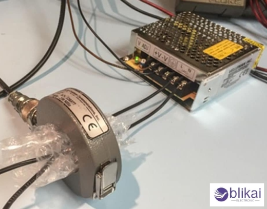
A. Use of Common Mode Chokes
Common-mode choke inductors Toroid or ferrite-core inductors are wound and optimized to offer very high resistance to common-mode currents, and near zero resistance to differential currents.
How They Work:
When a differential signal travels to both windings in opposite directions, the two magnetic fields cancel each other so that the signal can travel further.
When the signal is in common mode, fields will reinforce one another, resulting in high inductive impedance, causing noise suppression.
Applications:
AC line filters in switching power supplies
USB and HDMI ports in consumer devices
Ethernet transformers in networking equipment
Design Tip: Common-mode chokes should always be placed as much closer as possible to connectors/entry points to avoid noise propagation within the board.
B. PCB Design Best Practices
A significant portion of CMN issues stems from improper PCB layout. Following these layout strategies can dramatically reduce CMN:
- Tight coupling: Keep signal and return paths closely coupled to reduce loop area.
- Ground planes: Use continuous solid ground planes under signal traces to ensure low impedance return paths.
- Differential routing: For high-speed interfaces (e.g., USB, LVDS), use matched impedance differential pairs to maintain signal balance.
- Avoid stubs and abrupt trace transitions: These can act as antennas and exacerbate EMI.
Design Tip: Test your PCB layout with EMI/EMC simulators prior to making so as to determine areas of possible trouble spots.
C. Shielding and Grounding Strategies
The basic practices used to control the EMI and CMN are shielding and grounding.
Shielding:
Use shielded twisted pair (STP) cables for signal transmission.
Enclose sensitive circuits in metal enclosures connected to chassis ground.
Apply PCB-level shields over high-frequency components.
Grounding:
Use star grounding to prevent current from flowing between different parts of the system through shared paths.
Separate analog and digital grounds on mixed-signal boards and connect them at a single point.
Ensure low impedance paths from the chassis to earth ground.
Tip: In high-speed or high-sensitivity applications never daisy-chain grounds because this creates a ground loop that leads to the build up of CMN.
D. Filtering Techniques
Filtering is essential in both power and signal lines to suppress unwanted frequencies:
- Y-capacitors: Connect between the line and ground to divert common-mode noise to the chassis ground.
- Ferrite beads: Provide frequency-dependent resistance to high-frequency noise on power supply rails or signal lines.
- LC or π-filters: Create low-pass filters that attenuate CMN and conduct noise at specific frequency ranges.
Component Selection Note: Choose filter components with the correct current rating and impedance characteristics for your system’s frequency range.
Component Selection for Noise Reduction
Components used are very important in the immunity of a system to CMN. Consider:
- Low-EMI switching regulators with controlled slew rates and spread-spectrum modulation
- Optical isolators (optocouplers) to eliminate electrical continuity between noisy and quiet domains
- Isolation amplifiers for analog signal interfaces across ground domains
- EMI-suppressing connectors and shielded cables
Also, make sure there are decoupling capacitors near to IC power pins, then they can absorb the transients and lessen the noise coupling onto the board.
Real-World Examples and Applications
Industrial Control Systems
PLCs, sensor networks and variable frequency drives (VFDs) tend to work within electrically noisy environments. Galvanic isolation, shielding and common-mode filters are essential.
Medical Electronics
Electronics like ECG machines and infusion pumps should observe stringent levels of noise to guarantee the safety of patients and valid information. EMC specifications, such as Design according to IEC 60601, frequently determine the design.
Audio and Video Equipment
CMN causes audible pops, hums, and artifacts in the image. Balanced audio lines, shielding and isolation transformers support signal quality.
Automotive Systems
CMN results in audible hums, pops, and image artifacts. Balanced audio lines, shielding, and isolation transformers help maintain signal quality.
Testing and Troubleshooting Common Mode Noise
Efficient CMN mitigation depends on accurate diagnosis. Use the following tools:
- Differential and high-CMRR probes with oscilloscopes to detect CMN between conductors
- Clamp-on current probes to measure common-mode currents in cables
- Spectrum analyzers with LISNs (Line Impedance Stabilization Networks) for conducted EMI testing
- Near-field EMI probes to locate PCB hotspots emitting CMN
Also, consider pre-compliance EMI testing during design to avoid surprises during final certification.
Summary and Best Practices Checklist
Here’s a comprehensive checklist for reducing CMN:
- Identify and isolate noise sources
- Use common-mode chokes on data/power lines
- Implement shielded enclosures and cables
- Design PCBs with tight signal-return paths
- Separate analog and digital grounds
- Apply filtering at connectors and entry points
- Choose EMI-conscious components
- Test and verify with EMI tools early
By adopting the mentioned practices in your working process, you will be able to come up with high noise-resistant systems that will be easy to survive through or to undergo EMI tests without failures in the real operational world.
FAQ
1. What is common-mode noise, and how is it different from differential noise?
Common mode noise is the signal which is present on two or more conductors compared with ground as opposed to differential signals which are signals which appear on both but flow in opposite directions and bear the actual data.
2. How do I measure common-mode noise in my PCB?
Common-mode current through cables or ground loops can be measured using a differential oscilloscope probe between signal lines, or a clamp-on current probe.
3. Can ferrite beads eliminate common-mode noise?
Ferrite beads help in removing the noise generated at high frequency, but, used with good grounding, shielding measures and wiring skills, it is most effective.
4. What’s the best filter for reducing CMN in power supply lines?
Common-mode chokes paired with Y-capacitors provide an excellent combination to suppress high-frequency CMN on both AC and DC power lines.
Related Articles
Network Layer In OSI Model (Fully Explained)
Optical Line Protection in Modern Networks: Full Guide
Fiber Modems: Types, Advantages & Applications
Vacuum Tubes: Complete Guide to Types, Applications & Modern Roles
Some images are sourced online. Please contact us for removal if any copyright concerns arise.


