


MOSFET : Principle and Its Applications
The MOSFET (Metal Oxide Semiconductor Field Effect Transistor) is a semiconductor component extensively employed for switching operations and the amplification of electronic signals in various electronic devices. A MOSFET can be a core or part of an integrated circuit, designed and manufactured within a single chip due to its availability in extremely small dimensions. The advent of the MOSFET has significantly transformed the field of electronic switching. Let's proceed with a comprehensive explanation of this concept.
What is MOSFET?
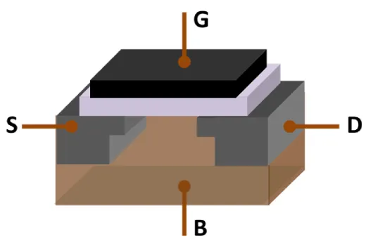
A MOSFET is a four-terminal component consisting of source (S), gate (G), drain (D), and body (B) terminals. Generally, the body of the MOSFET is connected to the source terminal, thus forming a three-terminal device similar to a field-effect transistor. MOSFETs are typically regarded as transistors and are used in both analog and digital circuits. This serves as a fundamental introduction to MOSFETs, and the typical structure of this device is illustrated below:
Based on the MOSFET structure outlined above, the operation of MOSFETs relies on electrical fluctuations occurring in the channel width, coupled with the movement of carriers (either electrons or holes). Charge carriers ingress the channel via the source terminal and egress through the drain.
The channel width is modulated by the voltage applied to an electrode known as the gate, positioned between the source and drain terminals. This gate is insulated from the channel by an exceedingly thin layer of metal oxide. The MOS capacitance within the device constitutes the pivotal segment governing its overall functionality.
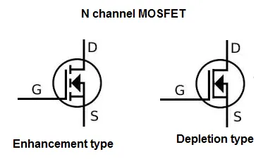
A MOSFET can operate in two modes:
Depletion Mode
Enhancement Mode
Depletion Mode
When there is no voltage applied to the gate terminal, the channel exhibits its highest conductance. However, when a voltage, either positive or negative, is applied to the gate terminal, the channel's conductivity diminishes. Please refer to this link to know more about Depletion Mode MOSFET.
Enhancement Mode
In the absence of voltage at the gate terminal, the device remains non-conductive. When the maximum voltage is applied to the gate terminal, the device demonstrates increased conductivity.
Operating Principle of MOSFET
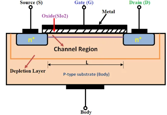
The fundamental principle underlying MOSFET functionality is its capability to regulate voltage and current flow between the source and drain terminals. It operates akin to a switch, with its functionality rooted in the MOS capacitor, which constitutes its primary component.
The semiconductor surface beneath the oxide layer, situated between the source and drain terminals, can undergo inversion from p-type to n-type by applying either positive or negative gate voltages, respectively. Upon applying a positive gate voltage, a repulsive force is generated, pushing the holes beneath the oxide layer downward into the substrate.
The depletion region is populated by bound negative charges associated with acceptor atoms. Upon electron arrival, a channel forms. The positive voltage also draws electrons from the n+ source and drain regions into the channel. Subsequently, when a voltage is applied between the drain and source, current flows unhindered between them, with the gate voltage governing electron behavior in the channel. Conversely, applying a negative voltage results in the formation of a hole channel beneath the oxide layer.
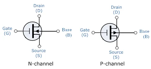
P-Channel MOSFET
The P-channel MOSFET features a P-channel region positioned between its source and drain terminals. Functioning as a four-terminal device, it encompasses gate, drain, source, and body terminals. The drain and source are heavily doped with p+ regions, while the body or substrate is of n-type, facilitating current flow in the direction of positively charged holes.
Application of a negative voltage with repulsive force at the gate terminal results in the downward displacement of electrons beneath the oxide layer into the substrate. The depletion region is populated by bound positive charges associated with donor atoms. Moreover, the negative gate voltage attracts holes from the p+ source and drain regions into the channel region.
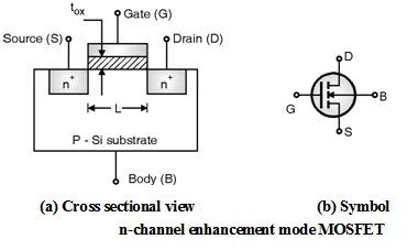
N-Channel MOSFET
The N-channel MOSFET incorporates an N-channel region positioned between its source and drain terminals. Like its counterpart, it operates as a four-terminal device, featuring gate, drain, source, and body terminals. In this variant of the Field Effect Transistor, the drain and source are heavily doped with n+ regions, while the substrate or body comprises P-type material.
Current flow in this MOSFET type occurs due to negatively charged electrons. Application of a positive voltage with repulsive force at the gate terminal prompts the downward movement of holes beneath the oxide layer into the substrate. The resulting depletion region is enriched with bound negative charges associated with acceptor atoms.
Upon electron arrival, a channel forms, with the positive voltage also enticing electrons from the n+ source and drain regions into the channel. Subsequent application of voltage between the drain and source enables unrestricted current flow, with the gate voltage regulating electron behavior within the channel. Conversely, application of a negative voltage leads to the formation of a hole channel beneath the oxide layer.
MOSFET Operating Regions
In its most general form, the operation of the MOSFET occurs primarily within three distinct regions:
Cut-off Region – This region signifies the device being in the OFF state, with zero current flowing through it. Here, the MOSFET acts as a basic switch, utilized when the need arises for electrical switching.
Saturation Region – Within this region, the device maintains a constant drain-to-source current regardless of any increase in the drain-to-source voltage. This occurs once the voltage across the drain-to-source terminals exceeds the pinch-off voltage threshold. Here, the MOSFET functions as a closed switch, allowing a saturated level of current to flow across the drain-to-source terminals. Hence, the saturation region is selected when the device is intended for switching operations.
Linear/Ohmic Region – In this region, the current across the drain-to-source terminal increases proportionally with the voltage across the drain-to-source path. MOSFETs operating within this linear region serve as amplifiers, facilitating signal amplification.
Now, let's delve into the switching characteristics of MOSFETs.
Both MOSFETs and Bipolar Junction Transistors (BJTs) serve as switches in two states: ON and OFF. To comprehend this functionality, let's examine the ideal and practical characteristics of the MOSFET device.
Ideal Switch Characteristics
When a MOSFET functions as an ideal switch, it should exhibit the following properties:
1. In the ON condition, there should be no limitation on the current it can carry.
2. In the OFF condition, the device should be able to block voltage without any limitations.
3. When the device is in the ON state, the voltage drop across it should be zero.
4. The resistance in the OFF state should be infinite.
5. There should be no restrictions on the switching speed.
Practical Switch Characteristics
Since real-world applications extend beyond ideal scenarios, the practical operation of a MOSFET should exhibit these properties:
1. In the ON condition, the power handling capability should be limited, meaning the conduction current must be restricted.
2. In the OFF state, the device should still block voltage without limitations.
3. Switching between ON and OFF states for finite times limits the device's speed and functional frequency.
4. In the ON condition, the MOSFET will have minimal resistance, resulting in a forward voltage drop. Additionally, there will be a finite resistance in the OFF state, leading to reverse leakage current.
5. During practical operation, the device dissipates power in both ON and OFF states, as well as during transitions between these states.
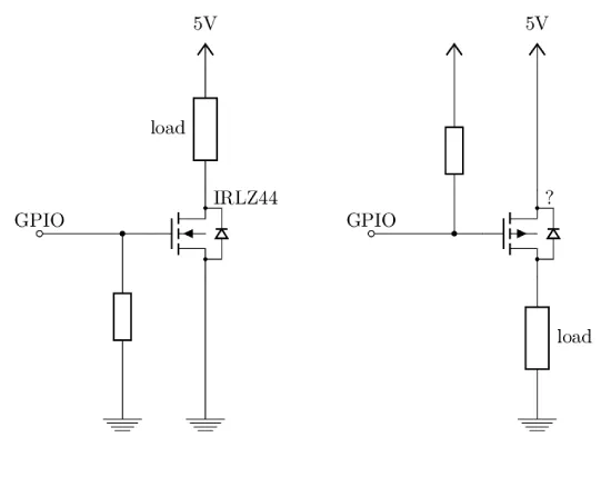
Example of MOSFET as a Switch
In the circuit arrangement depicted below, an enhancement-mode N-channel MOSFET is utilized to control the state of a sample lamp, toggling between ON and OFF conditions. Applying a positive voltage to the gate terminal triggers the transistor's base, illuminating the lamp in the ON state (where VGS = +v), while bringing the voltage level to zero transitions the device to the OFF state (where VGS = 0).
Should the resistive load of the lamp be substituted with an inductive load connected to a relay or diode, protective measures become imperative to safeguard the MOSFET device. While the illustrated circuit suffices for switching resistive loads like lamps or LEDs, additional protection is warranted when deploying MOSFETs as switches with inductive or capacitive loads.
Failure to protect the MOSFET may result in device damage. To function as an analog switching device, the MOSFET must transition between its cutoff region (where VGS = 0) and saturation region (where VGS = +v).
The MOSFET, serving as a transistor, is abbreviated as Metal Oxide Silicon Field Effect Transistor. Its nomenclature inherently denotes its transistor-like behavior, featuring both P-channel and N-channel variants. Configured with four terminals - source, gate, and drain - and connected in series with a resistive load of 24Ω, an ammeter, and a voltmeter, the device demonstrates its functionality.
Unlike bipolar junction transistors, where current flows across the base-to-emitter path, MOSFETs exhibit no current flow through the gate due to the presence of a capacitive element. Voltage alone suffices for operation.
This behavior is validated through simulation, toggling the switch ON/OFF. When the switch is ON, negligible current flows through the circuit. Connecting the 24Ω resistor and ammeter reveals minimal voltage drop across the source (+0.21V). The resistance between drain and source, denoted as RDS, causes voltage drop proportional to current flow, with RDS values varying (typically between 0.001, 0.005, and 0.05) based on device type.
For a comprehensive understanding of MOSFET functionality, experimentation with various MOSFET-based circuits listed below, either on a breadboard or at home, is recommended.
MOSFETs also offer the potential to construct Wireless Power Transfer (WPT) devices.
Key Concepts to Understand:
1) Selecting MOSFETs as Switches
Several considerations must be taken into account when choosing MOSFETs for switch applications:
Choice between P-channel or N-channel configurations
Maximum operating voltage and current ratings
Optimization of Rds ON, indicating the resistance at the Drain-to-Source terminal when the channel is fully open
Enhancement of operational frequency
Packaging options such as TO-220, DPAck, and others.
2) Understanding MOSFET Switch Efficiency
An essential aspect to consider when utilizing MOSFETs as switch devices is the maximum drain current capability. This is determined by RDS in the ON state, a critical parameter influencing the switching performance of the MOSFET. Represented as the ratio of drain-source voltage to drain current, it is calculated solely during the ON state of the transistor.
3) Why is a MOSFET Switch Used in a Boost Converter?
A boost converter generally requires a switching transistor for its operation, and MOSFETs are commonly used for this purpose. They are preferred because they can effectively manage current and voltage values, and their switching speed and cost-efficiency make them widely utilized.
Similarly, MOSFETs can be employed in various applications, such as:
- MOSFET as a switch for LED
- MOSFET as a switch for Arduino
- MOSFET switch for AC load
- MOSFET switch for DC motor
- MOSFET switch for negative voltage
- MOSFET as a switch with Arduino
- MOSFET as a switch with a microcontroller
- MOSFET switch with hysteresis
- MOSFET as switch diode and active resistor
- MOSFET as a switch equation
- MOSFET switch for airsoft
- MOSFET as switch gate resistor
- MOSFET as a switching solenoid
- MOSFET switch using an optocoupler
- MOSFET switch with hysteresis
Application of MOSFET as a Switch
An exemplary application of the MOSFET as a switch is in automatic brightness control for streetlights. Modern highway lights often utilize high-intensity discharge (HID) lamps, which consume significant energy. However, controlling the brightness of HID lamps based on requirements poses challenges.
To address this issue, an alternative lighting method using LEDs can be implemented. LEDs offer advantages over HID lamps, such as customizable brightness levels. The primary objective is to directly control highway lights using a microprocessor.
This can be achieved by adjusting clock pulses, allowing the device to switch lamps as needed. The system incorporates a Raspberry Pi board equipped with a processor for management. LEDs replace HIDs and are connected to the processor via MOSFETs. The microcontroller adjusts duty cycles and signals the MOSFET to provide varying levels of intensity.
Advantages:
- Enhanced efficiency even at low voltage levels
- Absence of gate current leads to higher input impedance and increased switching speed
- Minimal power and current usage
Disadvantages:
- Instability when operated at overload voltage levels
- Thin oxide layer may be susceptible to damage from electrostatic charges
Applications
The versatility of MOSFETs finds application in various fields:
- MOSFET-based amplifiers excel in high-frequency applications.
- These devices regulate DC motors efficiently.
- Their superior switching speeds make them ideal for chopper amplifier construction.
- MOSFETs serve as passive components in diverse electronic elements.
In summary, while transistors demand current, MOSFETs operate on voltage. The driving requirements for MOSFETs are simpler and more efficient compared to BJTs.
Related Articles
Impact of IRF3205 MOSFET on Power Electronics: Advancements and Applications
IRF3205 MOSFETs: Applications, Features, and Equivalent


