


NPN Transistor? Construction, Working & Applications
 NPN Transistor
Amplification, switching, and signal processing are all possible with NPN transistors, which are essential semiconductor devices. Electronics enthusiasts must understand how they are built, how they function, and what they are used for. From their layered semiconductor structure to their pivotal role in modern technology, this introduction sets the stage for exploring the intricacies of NPN transistors.
What are NPN Transistors?
In electronic circuits, NPN transistors are classified as bipolar junction transistors (BJTs), which are often used for signal processing, amplification, and switching. A transistor is called "NPN" because of its semiconductor layers arranged in a pyramidal pattern. A NPN transistor is constructed from two layers of N-type semiconductors sandwiched between P-type semiconductors. With this configuration, a small current is applied to the base terminal in order to control the flow of current between the collector and emitter terminals.
A small current can flow from the collector to the emitter of an NPN transistor by applying a small current to its base terminal. The forward bias of PN junctions allows current to flow across them, while the reverse bias prevents current from flowing across them. Since NPN transistors can efficiently control and amplify electrical signals, they are prominent in electronic devices such as amplifiers, switches, oscillators, and voltage regulators.
Working Principle of NPN Transistor
In order to understand how transistors form their three regions, it is necessary to understand that doping is the process by which they are grown. Different doping concentrations are used in these regions to achieve functionality. Boron, a trivalent element, is concentrated in the base region, forming a few holes. With phosphorus, a pentavalent element, a medium concentration of free electrons is formed in the collector region. There are many free electrons in the emitter region due to the heavy phosphorus doping. The junctions, however, prevent free electrons from flowing into the base due to their confinement.
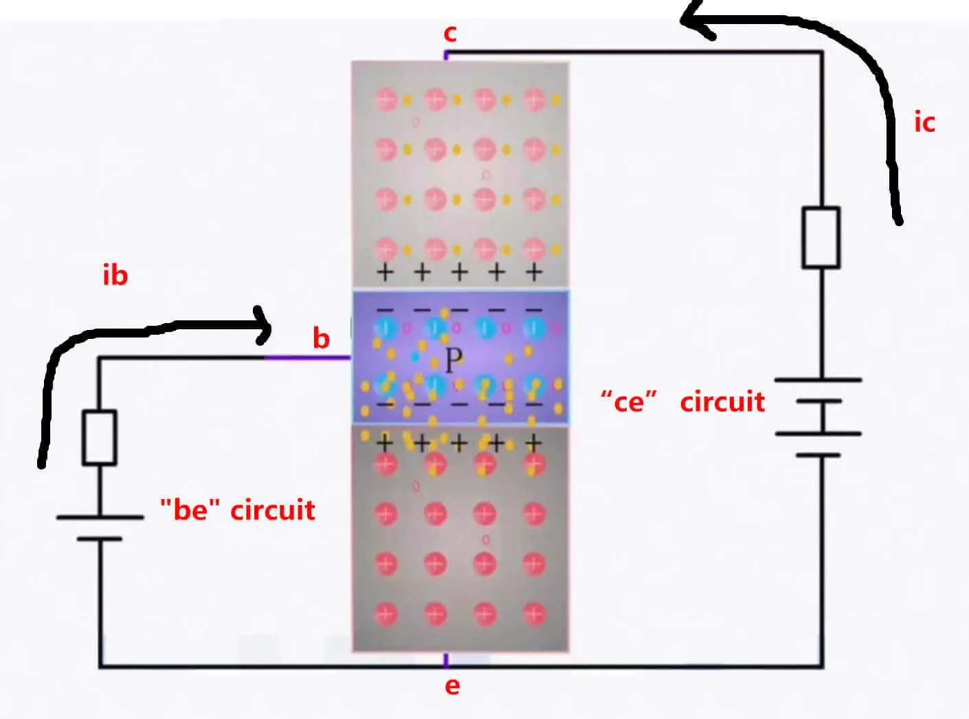
It is necessary for free electrons to move in order to enable amplification. What is the working principle of a NPN transistor? Below is a circuit diagram with an NPN transistor attached to a circuit that includes two circuits labeled "BE" and "CE."
 Working Principle of NPN Transistor
A forward-biased diode (mentioned earlier in the analogy) is in the circuit "be". In this state, free electrons are able to diffuse from the emitter region to the base region due to the external electric field overpowering the internal electric field. In the diffused region of the emitter, free electrons exhibit two states:
-
Free electrons in the base region combine with holes.
-
During the collector region, a large amount of free electrons flow.
With decreasing base holes, the external circuit replenishes them, creating a current "ib," which is created by free electrons. "ic/ib" remains constant as "ic/ib" decreases. NPN transistors control the flow of current between collectors and emitters through a base current. The following conditions must be met, however:
-
It must be greater than 0 volts to be considered a base current
-
Ideally, the collector and emitter should be separated by a voltage difference of at least 0.2 volts.
Construction
NPN transistors consist of three layers, two of which are N-type semiconductors, and one of which is P-type semiconductors. When two diodes are connected back to back, they form a transistor. However, it is only used to visualize the construction.
Two diodes connected back to back contain two doped regions each, so a structure created by connecting them back to back will have four doped regions. It is therefore impossible to form a transistor based on a back-to-back connection when uniform doping is not present.
Hence, it always consists of three layers, a base with light doping, an emitter with heavy doping, and a collector with moderate doping. It sandwiched the emitter and collector of N-type between the base of P-type. N-type semiconductors are formed as a result.
Is it possible to interchange emitters and collectors?
Due to the size difference between the emitter and collector regions, the emitter cannot be used interchangeably with the collector. It is designed with a larger collector than an emitter since a larger collector will collect more and more charge carriers, while a larger junction will also easily dissipate heat.
NPN Transistor Applications
Electronic circuits require NPN transistors, which can be found in a range of applications. We explore their various uses in detail here:
Amplification: An extensive use of NPN transistors in amplification circuits can be found in the boosting of weak electrical signals. Transistors enhance input signals by conducting a much larger current from the collector to the emitter when a small current or voltage is applied to the base terminal. Since NPN transistors have this property, they are crucial for audio amplifiers, which boost speaker and headphone sound.
Switching: Electronic circuits commonly use NPN transistors as switches. An NPN transistor turns circuits on and off by controlling the flow of current between its collector and emitter terminals. An electric current can flow freely from collector to emitter when a sufficient voltage is applied to the transistor's base terminal. Power switches, relay drivers, and digital logic gates often use NPN transistors.
Oscillation: The NPN transistor is an important component of oscillator circuits that generate periodic waveforms like sine waves, square waves, and triangular waves. A feedback loop incorporating NPN transistors allows oscillators to maintain a continuous oscillation at a certain frequency. They are used in RF communication systems, clock generators, and audio synthesizers, among other applications.
Voltage Regulation: Despite fluctuations in input voltage or load conditions, NPN transistors are essential components of voltage regulator circuits that stabilize power supply output voltages. NPN transistors use series pass elements (such as resistors or transistors) in order to maintain a constant output voltage. In order to prevent damage from voltage spikes or dips, it is vital to ensure stable device operation.
Signal Processing: Many applications of NPN transistors can be found in signal processing, including filtering, modulation, and signal conditioning. Using NPN transistors, relevant information can be extracted, noise can be reduced, or frequencies can be modulated by manipulating input signals. Sensor systems, audio processing equipment, and telecommunications all require these capabilities.
Temperature Sensing: Temperature sensors can be created using NPN transistors. With transistors, changes in temperature can be measured accurately by utilizing their base-emitter voltages, which are temperature-dependent. It is typically used to monitor temperatures in industrial processes, to monitor the environment, and to protect electronic equipment.
Faqs
Question 1: How do NPN transistors fail? What are some common issues?
Answer: Collector current can increase due to thermal runaway, voltage can drop at saturation (VCE saturation), and breakdowns are common due to overvoltage or overcurrent conditions. Thermal management techniques, heat sinking, and voltage/current limiting can mitigate these problems.
Question 2: What are the differences between NPN and PNP transistors?
Answer: Semiconductor layers are arranged differently. Emitters in NPN transistors are N-type, while emitters in PNP transistors are P-type. Consequently, biasing requirements and current flow directions differ. The collector of an NPN transistor is typically connected to the emitter while the emitter of a PNP transistor is typically connected to the collector.
Wrapping Up
NPN transistors offer unparalleled functionality and versatility in the world of electronics. A myriad of applications have made it indispensable as an amplifier and switch. With high current gains, NPN transistors are able to efficiently amplify signals by controlling the flow of charge carriers from the emitter to the collector. In addition to this characteristic, integrated circuits are small and cost-effective, enabling them to be designed into any electronic device. NPN transistors can be found in a wide range of electronic systems, from audio amplifiers to digital logic gates.
In addition, designers must deal with the transistor's limitations, such as the finite saturation voltage and the vulnerability to overcurrents and overvoltages, in order to ensure that the transistor performs efficiently and reliably. Modern electronics rely heavily on NPN transistors, despite these challenges, driving innovation and enabling technological advancement across a wide range of industries.
Related Articles
BC338 NPN Transistor: Features, Applications, and FAQ
2N4401 NPN Transistor: Datasheet, Applications, and Features


