


Phototransistor : Circuit Pinout & Principle
The concept of a phototransistor has been known for many years. It was first proposed by William Shockley in 1951, shortly after the discovery of the normal bipolar transistor. Two years later, a working phototransistor was demonstrated and it has since been used in various applications. Its development has continued over time and today, phototransistors are readily available at low cost from electronic component distributors for use in different electronic circuits. A phototransistor is a type of semiconductor device that detects light levels and modifies the current flow between its emitter and collector terminals based on the amount of light it receives. This article provides an overview on phototransistors.
What is a Phototransistor?
A Phototransistor is an electronic component that functions as a switch and current amplifier, relying on light exposure to operate. When the junction is exposed to light, there is a proportional flow of reverse current. Phototransistors are widely used for detecting light pulses and converting them into digital electrical signals. Unlike conventional transistors, they are controlled by light rather than electric current. These phototransistors offer high gain and are cost-effective, making them suitable for various applications.

What is a Phototransistor?
A Phototransistor is an electronic component that converts light energy into electric energy. It operates similarly to a photoresistor, also known as an LDR (light dependent resistor), but it can generate both current and voltage, unlike the photoresistor which only produces current due to changes in resistance.
Phototransistors have their base terminal exposed, and instead of sending current into the base, they are activated by photons from incoming light. This is because phototransistors are made of a bipolar semiconductor that focuses on the energy transmitted through it. They are activated by light particles and are used in various electronic devices that rely on light.
All silicon photosensors, including phototransistors, respond to the entire visible radiation range as well as infrared. In fact, all diodes, transistors, Darlington's, TRIACs etc., have the same fundamental radiation frequency response.
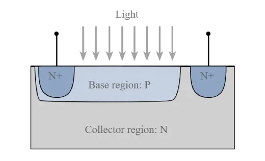
The structure of a phototransistor is specifically designed for photo applications. It has a larger base and collector width compared to a regular transistor and is manufactured using diffusion or ion implantation techniques.
Construction of Phototransistor
The construction of a phototransistor involves using an ordinary bi-polar transistor with the base region exposed to illumination. It comes in both P-N-P and N-P-N types, with configurations such as common emitter, common collector, and common base, although the common emitter configuration is typically preferred. It can also function with an open base. In comparison to a standard transistor, it has larger base and collector areas.
Historically, phototransistors were made using single semiconductor materials, such as silicon and germanium. However, modern components now use materials like gallium and arsenide to achieve higher efficiency levels. The base serves as the lead that activates the transistor and acts as the gate controller device for the larger electrical supply. The collector is the positive lead responsible for organizing the larger electrical supply, while the emitter is the negative lead serving as an outlet for the larger electrical supply.
In the absence of light, a small current flow occurs in the phototransistor due to thermally generated hole-electron pairs. As a result, the output voltage from the circuit is slightly lower than the supply value due to the voltage drop across the load resistor R. However, when light falls on the collector-base junction, the current flow increases. If there is an open circuit at the base connection, then the collector-base current must flow in the base-emitter circuit. This leads to amplification of current through normal transistor action.
The collector-base junction of a phototransistor is highly sensitive to light and its operation depends on light intensity. The base current produced by incident photons is amplified by transistor gain, resulting in current gains ranging from hundreds to several thousand. In terms of sensitivity and noise levels, a phototransistor is 50 to 100 times more sensitive than a photodiode.
A phototransistor operates similarly to a regular transistor, with emitter, base, and collector terminals. The collector terminal is positively biased in relation to the emitter terminal, while the BE junction is reverse-biased.
In a phototransistor, light striking the base terminal activates the device and allows for the generation of hole-electron pairs and current flow across the emitter or collector. As current increases, it becomes concentrated and converted into voltage.
Typically, a phototransistor does not have a base connection. Instead, light enables current flow throughout the phototransistor without requiring a connection at the base terminal.
Types of Phototransistor
Phototransistors can be categorized into two types, namely BJT and FET.
BJT Phototransistor
In the absence of light, a BJT phototransistor allows for leakage between the collector and emitter at a low level of around 100 nA. However, when exposed to light, it can handle currents up to 50mA. This sets it apart from a photodiode that has a lower current capacity.
FET Phototransistor
This type of phototransistor has two terminals that connect internally through its collector and emitter or source and drain in the case of an FET. The base terminal of the transistor responds to light and controls the flow of current between the terminals.
Phototransistor Circuit
A phototransistor functions similarly to a regular transistor, amplifying base current to produce collector current. The difference lies in how the base current is controlled by visible or infrared light. Additionally, unlike traditional transistors, a phototransistor only requires two pins for operation.
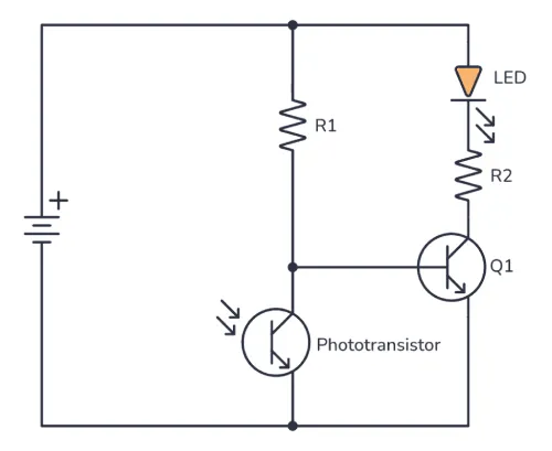
In a basic circuit, if Vout is not connected to anything, the collector current, which flows through the resistor, will be determined by the base current controlled by the level of light. As a result, the voltage at Vout will fluctuate based on the intensity of light. This output can be connected to an op-amp to amplify the signal or directly to an input of a microcontroller.
The output of a phototransistor relies on the wavelength of incoming light. These devices are sensitive to light spanning from near UV through visible and into near IR parts of the spectrum. Under a specific illumination level from a given light source, their output is determined by both the area of their exposed collector-base junction and their dc current gain.
Phototransistors come in various forms including optoisolators, optical switches, and retro sensors. An optoisolator resembles a transformer as its output is electrically isolated from its input. The optical switch detects an object entering its gap and obstructing light between its emitter and detector. Meanwhile, retro sensors identify objects by emitting light that reflects off them for sensing purposes.
Amplification:
The functioning range of a phototransistor primarily relies on the intensity of the incident light as it is controlled by the input at the base. The current from incident photons received at the base terminal can be amplified through the transistor's gain, resulting in a current gain ranging from 100 to 100. Compared to a photodiode, a phototransistor has higher sensitivity with less noise level.
Additional amplification can be achieved through a photodarlington-type transistor.
This type of phototransistor consists of an emitter output connected to the base terminal of another bipolar transistor. It offers high sensitivity in low light conditions as it provides a current gain equivalent to that of two transistors. The combined gain from these two stages can reach values exceeding 100,000A. However, a photodarlington transistor exhibits lower response compared to a standard phototransistor.
Modes of Operation:
In phototransistor circuits, there are two main modes of operation: active and switch. The most commonly used mode is switch type, which exhibits non-linear response to light; when there is no light, there is no flow of current through the transistor. As exposure to light increases, current starts flowing. Switch mode operates in an ON/OFF system.
Active mode, also known as linear mode, responds proportionally to the stimulus provided by light.
Performance Specifications
The choice of a phototransistor depends on various parameters and specifications, including the following.
- Collector Current (IC)
- Base Current (Iλ)
- Peak Wavelength
- Collector-to-Emitter Breakdown Voltage (VCE)
- Collector-emitter breakdown voltage (VBRCEO)
- Emitter-collector breakdown voltage (VBRECO)
- Dark current (ID)
- Power dissipation (PD or Ptot)
- Rise time (tR)
- Fall time (tF)
Design Parameters
The sensitivity of this type of transistor is influenced by the selected materials and composition. Homo-structure or single material devices typically have gain levels ranging from 50 to several hundred and are often designed with silicon. Heterostructure devices or those with multiple material configurations may have gain levels up to 10k, but they are less common due to high production costs.
Different materials have varying electromagnetic wavelength ranges:
- Silicon (Si) material: 190 to 110 nm
- Germanium (Ge) material: 400 to 170 nm
- Indium gallium arsenide (InGaAs) material: 800 to 260 nm
- Lead sulfide material: <100 to 350 nm
Mounting technology plays a crucial role in the proper functioning of a phototransistor.
Surface mount technology involves soldering component terminals onto a PCB using solder and flux formulation. The PCB pads are usually coated with paste, and high temperatures from an infrared oven dissolve the paste to solder the component terminals onto the PCB pads.
Through-hole technology (THT) is commonly used for mounting components. This involves placing component terminals through holes in the PCB and soldering them on the opposite face of the PCB. Phototransistors often feature a cutoff filter to block visible light, while some may have improved light detection through an anti-reflective coating. Additionally, devices with a round dome lens instead of a flat lens are also available.
Photodiode vs Phototransistor
The distinction between photodiode and phototransistor includes the following.
| photodiode | phototransistor |
| A photodiode is a PN-junction diode that produces electric current when struck by a photon of light. | The phototransistor is utilized to convert the energy of light into electrical energy. |
| It has lower sensitivity. | It has higher sensitivity. |
| The output response of the photodiode is quick. | The output response of the phototransistor is slow. |
| It produces current. | It produces voltage and current. |
| It is used in solar power generation, detecting UV or IR rays, and for light measuring, among other applications. | It is used in compact disc players, smoke detectors, lasers, invisible light receivers, and more. |
| It has a higher sensitivity to incident lights. | It has a lower sensitivity. |
| The dark current of the photodiode is reduced. | Phototransistor has a higher dark current. |
| In this, both forward and reverse biasing are used. | In this, only forward biasing is used. |
| The linear response range of photodiode is much wider. | The linear response range of phototransistor is much narrower. |
| Photodiode allows low current as compared to a phototransistor. | Phototransistor allows high current as compared to the photodiode. |
| The photodiode is used for battery-powered devices that use less power. | The phototransistor is used as a solid-state switch, different from the usage of a photodiode. |
Features of the Phototransistor
The phototransistor possesses the following characteristics.
- Affordable visible and near-IR photodetection.
- Gains ranging from 100 to over 150.
- Moderately quick response times.
- Available in various packages, such as epoxy-coated, transfer-molded, and surface mounting technology.
- Electrical traits similar to those of signal transistors.
Advantages of Phototransistor
Phototransistors offer several key advantages that distinguish them from other optical sensors, some of which are highlighted below.
- Phototransistors generate a higher current compared to photodiodes.
- They are relatively affordable, straightforward, and compact enough to accommodate multiple units on a single integrated computer chip.
- They operate very swiftly and can deliver nearly instantaneous output.
- Unlikе photo-resistors, phototransistors produce voltage.
Disadvantages of Phototransistor
- Silicon-based phototransistors cannot handle voltages exceeding 1,000 Volts.
- They are also more susceptible to electrical surges and spikes as well as electromagnetic energy.
- Furthermore, they do not allow electrons to move as freely as other devices like electron tubes.
Applications of Phototransistors
Phototransistors are used in various applications including:
- Punch-card readers.
- Security systems
- Encoders for measuring speed and direction.
- IR detectors for photoelectric controls.
- Computer logic circuitry.
- Relays
- Lighting control (e.g., highways)
- Level indication
- Counting systems
In conclusion, phototransistors are widely employed in electronic devices for light detection, such as infrared receivers, smoke detectors, lasers, CD players, etc. Lastly, what is the distinction between a phototransistor and a photodetector?
Related Articles
Varieties of Monitor Cables: A Beginner's Guide
Transistor Series Voltage Regulator:All You Need to Know
Junction Field-Effect Transistors: Principles, Applications, and Advantages


