


Junction Field-Effect Transistors: Principles, Applications, and Advantages
What is Junction Field-Effect Transistors (JFETs)?
Junction Field- Effect Transistors( JFETs) are a type of transistor used to control the inflow of current in electronic circuits. Unlike bipolar junction transistors( BJTs) that use current to control current, JFETs use voltage to regulate current inflow, making them part of the larger family of field- effect transistors( FETs). A JFET consists of three main outstations the Gate, Source, and Drain. The device operates by creating an electric field that controls the conductivity of a channel, which can be either n- type or p- type. This characteristic allows JFETs to offer high input impedance and low noise situations, making them ideal for a variety of sensitive electronic operations. Their simplicity and effectiveness have made them a chief in analog and digital circuits since their development in themid-20th century.
.webp)
Principles of Junction Field-Effect Transistors
A. Basic Structure and Components
Electric current can be controlled via a type of transistor called a junction field effect transistor (JFET). It consists of three main terminals:
1. Gate (G):
The current flow between the source and drain is managed by the gate terminal. Reverse bias is what this is. This indicates that, in typical functioning circumstances, it won't require electricity.
2. Source (S):
The source terminal is the origin point of the current that flows through the JFET. It provides the carriers (electrons for n-channel, holes for p-channel) for current flow.
3. Drain (D):
The drain terminal is where the current exits the JFET after passing through the channel.
B. Operating Mechanism
The gate-to-source voltage creates an electric field that JFETs use to function. The following ideas will help you comprehend how a JFET regulates the conductivity of the channel between the source and drain:
1. Depletion Mode Operation:
- Depletion mode refers to the JFET's initial state, when no voltage is provided to the gate. Between the source and the drain in this mode, there is a conducting channel. to permit unrestricted stream flow.
- When the gate receives an applied negative voltage (for n-channel JFETs) or positive voltage (for p-channel JFETs). The channel will be used by the carrier. There is a decrease in the channel width. and hence, the current flow.
2. Voltage Control of Current Flow:
- The current flow from the source to the drain (I_D) is controlled by the voltage applied to the gate (V_GS). A more negative V_GS (for n-channel JFETs) narrows the channel, reducing I_D. Conversely, a less negative V_GS or a positive V_GS widens the channel, increasing I_D.
- There is a threshold voltage (V_GS(th)) at which the channel becomes completely pinched off, and current flow stops. This is called the pinch-off voltage.
C. Key Characteristics
1. High Input Impedance:
The JFET has a very high input impedance. Generally speaking, they range from gigaohms (GΩ) to megaohms (MΩ). The reverse biased and low current consumption of JFETs makes them perfect for the input stage of electrolytic amplifiers.
2. Low Noise Level:
JFETs are renowned for having low noise levels. Because of this, they can be used in sensitive signal processing circuits like low noise amplifiers and audio outfit and instrumentation.
Types of Junction Field-Effect Transistors (JFETs)
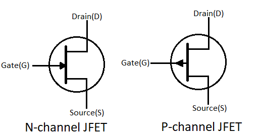
A. N-channel Junction Field-Effect Transistors (JFETs)
One of the two types of JFETs that is distinguished by the movement of electrons acting as charge carriers is the N-channel JFET. Here are the key features and characteristics:
1. Structure:
- N- type semiconductor material is used to produce the depression.
- The gate and channel form a p-n junction since the gate is composed of p-type material.
2. Operation:
- The reduction region widens when the gate-to-gate voltage(V_GS) is negative. lowers the current inflow from source to drain(I_D) by narrowing the channel.
- Whether V_GS is positive or zero. It will be a fully open channel. lets the most current flow through.
3. Key Characteristics:
- Electrons have greater mobility than holes do. Resistance is reduced and electrical conductivity is raised as a result.
- Transition conductor gain (gain) of n-channel JFETs is often higher than that of p-channel JFETs.
- More common in practical applications due to better performance characteristics.
B. P-channel Junction Field-Effect Transistors (JFETs)
A contrasting variety of JFET known as the P-channel JFET is distinguished by flowing holes acting as charge carriers. Here are the key features and characteristics:
1. Structure:
- P-type semiconductor material is used to create the cavity.
- The gate's n-type construction forms a p-n junction with the channel.
2. Operation:
- A advanced reduction region is observed when the gate- to- source voltage(V_GS) is positive. lower the current inflow from the source to the drain(I_D) by narrowing the channel.
- When V_GS is negative or zero. It will be a fully open channel. lets the most current flow through.
3. Key Characteristics:
- Compared to electron movement, hole movement is less. As a result, resistance is higher than with n-channel JFETs.
- Through-conductance (gain) of p-channel JFETs is typically lower than that of n-channel JFETs.
- Because of their comparatively low performance indicators, they are not frequently used in applications.
C. Comparison of N-channel and P-channel Characteristics
There’s a comparison of the characteristics of n- channel and p- channel JFETs:
|
Characteristic |
N-channel JFET |
P-channel JFET |
|
Channel Type |
n-type semiconductor |
p-type semiconductor |
|
Charge Carriers |
Electrons |
Holes |
|
Gate Voltage (V_GS) |
Negative to reduce current |
Positive to reduce current |
|
Mobility |
Higher (better conductivity) |
Lower (higher resistance) |
|
Transconductance |
Higher (greater gain) |
Lower (less gain) |
|
Commonality |
More commonly used |
Less commonly used |
|
Resistance |
Lower |
Higher |
Applications of Junction Field-Effect Transistors (JFETs)
A. Amplifiers
JFETs are frequently found in several kinds of amplifiers. because of their low noise properties and high input impedance.
1. Low-noise amplifiers:
When it comes to sensitive applications like radios, microphones, and medical equipment, JFETs are the perfect choice for low-noise amplifiers (LNAs) since they generate less noise than bipolar junction transistors (BJTs).
2. Operational amplifiers:
JFETs are employed in the input stage of functional amplifiers( op amps) to produce low offset voltage and high input impedance. This guarantees a low position of noise in the input signal. For precision applications, JFET-based op amps are hence appropriate.
B. Switches
JFETs can act as analog switches due to their capability to control current inflow with a gate voltage.
Analog switches:
In situations where low on resistance and high off resistance are required, JFETs can be employed to switch analog signals. detected in sample circuits and tend to freeze. circuit with a multiplexer and chopper.
C. Voltage-controlled Resistors
In some arrangements, JFETs can function as voltage-controlled resistors.
Variable resistors:
By using JFETs in the ohmic region (where they act like a resistor) the resistor can be controlled by the gate-to-gate voltage (V_GS), making JFETs useful in applications requiring adjustable resistance, such as volume control and automatic gain control circuits (AGC).
D. Oscillators
JFETs are employed in oscillator circuits to generate periodic signals.
Oscillator circuits:
JFETs are utilized in oscillator circuits, such as LC oscillators and crystal oscillators, because of their high input impedance and low noise. Applications for these circuits include digital circuit clock production, communication systems, and signal generators.
E. Analog Signal Processing
In the processing of analog signals, the JFET is crucial. particularly in measurement tools and audio equipment.
1. Audio equipment:
JFETs are utilized in tone control circuits and preamplifiers in audio equipment. It contributes to the preservation of the audio signal's integrity because of its great sensitivity and low noise. This ensures sound reproduction of the highest caliber.
2. Instrumentation:
Sensor interfaces and measuring instruments are just two of the many instrumentation applications that use JFETs. Low leakage current and high input impedance are needed for this. This guarantees little signal distortion and precise signal processing.
Advantages of Using Junction Field-Effect Transistors (JFETs)
A. High Input Impedance Benefits
Minimal Signal Distortion:
The JFET can take in relatively little current from the signal source due to its high input impedance, which is typically in the mega-ohm to gigaohm range. By doing this, the loading impact is lessened and the input signal's integrity is preserved.
Ideal for Sensitive Applications:
Because of its high input impedance, the JFET is a good choice for operations like sensors and medical outfit that need to descry and amplify weak signals.
B. Low Noise Performance
Superior Signal Quality:
JFETs are a better fit for low-noise applications like preamplifiers because they produce less internal noise than BJTs. accuracy measurement apparatus and radio frequency amplifiers.
Enhanced Clarity:
The JFET's low noise performance guarantees the preservation of great fidelity and clarity in the amplified signal. This is crucial for precise analogue signal processing and high-end audio equipment.
C. Simple Biasing Requirements
Ease of Design:
When considering other transistor types, the bias circuit for a JFET is quite straightforward. Reverse bias exists in the gate. Additionally, the gate source voltage regulates the source's current. Circuit design is made simpler as a result.
Cost-Effective Implementation:
JFET-based circuits are an appealing solution for a variety of applications because of their easy biasing characteristic, which lowers the complexity and cost of implementation.
D. Robustness and Reliability
Thermal Stability:
The thermal stability of the JFET is good. This indicates that performance is constant across a temperature range. Its continuity makes it a dependable element in a range of settings.
Durability:
The essential design of JFETs provides a high position of continuity and resistance to damage fromover-voltage conditions, contributing to their long- term trustability in electronic circuits.
E. Energy Efficiency
Low Power Consumption:
Very little power is used by the JFET. This is due to the essentially insignificant gate current. The reverse bias in the gate-source connection is the reason for this. The JFET is energy-efficient because of this property. This is particularly valid for portable and battery-operated gadgets.
Optimal Performance:
JFET integrated circuits' overall power efficiency is enhanced by their low-power operation, making them advantageous in situations where energy conservation is crucial.
Related Articles
Thyristor vs Transistor: What are the Differences?


