


PNP Transistor? Construction, Working & Applications
Transistors are semiconductor devices. Many electrical circuits use it as a basic component. It is used as a switch or regulator in circuits due to its ability to regulate voltage or current. Electric signals can be controlled, amplified, or generated with it. Semiconductors of the P-type and N-type are used in most transistors. There are three layers of semiconductor in a PNP transistor: one N-type layer, one P-type layer, and one channel.
The FAQs below explain how the PNP transistor differs from the NPN transistor, as well as how it is constructed, how it works, and what it is used for.
What is a PNP Transistor?
An electronic circuit commonly uses a PNP transistor (also known as a BJT) for amplification or switching. Physisorption nanoparticles (PNP) are semiconductor layers arranged within transistors. PNP transistors have a P-type semiconductor sandwiched between two N-type semiconductors, forming two PN junctions. By applying a small current to the base terminal, a control current can be applied to the emitter and collector terminals to control current flow.
In contrast to NPN transistors, PNP transistors allow current to flow from the emitter to the collector by applying a small current to their base terminals. A PN junction is biased forward by forward bias, allowing current to flow across it, while a reverse biased junction prevents current from flowing across it. High-side switching or current amplification is often performed by PNP transistors in circuits in which the current is supplied from the collector to the emitter terminal.
PNP Transistor Construction and Symbol
Construction
PNP transistors consist of three regions: the emitter, the base, and the collector, which are constructed by layering different types of semiconductor materials. Electrical properties are usually created by doping these regions with specific impurities. The construction process is outlined below:
Emitter Region (P-type): Positively doped semiconductor material makes up the emitter, hence the "P" designation. Majority of the charge carriers (holes in P-type materials) are emitted from this region. Conduction through the transistor is accomplished by carriers.
Base Region (N-type): A negatively doped semiconductor material is used for the base, hence the "N" designation. Charge carriers flow between the emitter and collector in this region, which is very thin compared to the other regions. A small current or voltage is applied to the base to receive the input signal.
Collector Region (P-type): Another positively doped semiconductor material is used for the collector. A transistor's base creates the path for current to exit by carrying the majority of charge carriers (holes), which pass through its base during operation.
Symbol
A PNP transistor is represented in circuit diagrams by a standardized symbol. A transistor has three terminals: the emitter (E), the base (B), and the collector (C). When the transistor is in its active region, the arrow in the symbol indicates the direction of conventional current flow. The symbol is broken down as follows:
Emitter (E): An arrow points towards this terminal when the transistor is in the active region, indicating the direction of conventional current flow. A transistor's P-type region corresponds to this region.
Base (B): Controlling a transistor's operation is done through this terminal. In transistor construction, it represents the N-type region.
Collector (C): Flowing current through the transistor is collected at this terminal. A transistor's P-type region corresponds to this region.
The base and collector terminals of transistors do not have arrows on circuit diagrams, whereas the emitter terminal has an arrow pointing outward. An understanding of the PNP transistor can be gained from the arrangement of these terminals in the symbol.
Working of PNP Transistor
It works by forward biasing the emitter-base junction and reverse biasing the collector-base junction in PNP transistors. As the emitter terminal is made up of a P-type semiconductor, it must be connected to the positive terminal, while the N-type must be connected to the negative terminal in order to forward bias the semiconductor.
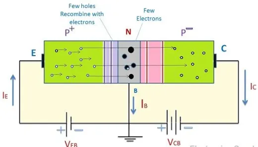
A negative terminal is connected to the P-type for reverse biasing collector-base junctions, while the positive terminal is connected to the N-type.
Emitter-base junctions will have narrow regions of depletion when biasing is applied, whereas collector-base junctions will have wide regions. Depletion layers are narrow due to forward bias at emitter-base junctions. The depletion width of the collector-base junction is wide because of the reverse biasing of the collector-base junction.
Effective base width Concept
In P-type semiconductors, holes dominate charge carriers, and in N-type electrons, electrons dominate charge carriers. Positive terminals of the battery will repel the hole in the emitter region, whereas electrons present in the N-region will attract it. As a result, both junctions have a reduced effective base width.
Emitter size and doping Effectiveness
A heavy doping is present on the emitter, which has a larger area than the base but a smaller one than the collector. There are fewer electrons in the base because it is lightly doped. In the emitter region, these few electrons combine with holes emitted by the positive terminal of the battery due to the repulsion from the positive terminal. Due to the small size and light doping of the base, only a few holes will combine with electrons present there.
There has been no interaction between electrons on the base terminal and electrons on the top terminal for the majority of electrons. There will be an electron flow towards the collector as a result of this. By being attracted by the negative terminal of the battery through which the collector is connected, they will move further towards the end of the collector region.
This circuit is powered by electric current flowing due to the movement of holes. The base current in the circuit is also generated by some holes located away from the base. The current will flow from the base and collector towards the emitter, while from the base and collector outwards. PNP transistors have the following equation for current.

PNP Transistor Applications
Due to their ability to switch circuits on and off, as well as amplify signals, PNP transistors find a wide range of applications in electronics. Here are a few common applications explained in detail:
Amplification: Transistors with PNP characteristics are commonly used to boost low-level input signals to higher levels in amplification circuits. In an amplifier circuit, the input signal controls the current flow between the emitter and collector by applying it to the base terminal of the PNP transistor. Input signals are amplified by modulating this current. An audio amplifier often uses PNP transistors to boost the strength of audio signals.
Switching: Switches in electronic circuits are also made up of PNP transistors. PNP transistors can control current flow between the collector and emitter terminals in order to turn on and off circuits. Transistors are turned on by passing current from the base terminal to the emitter and collector when a small current is applied to the base terminal. PNP transistors are useful for applications such as relay drivers, logic gates, and power switches because of this property.
Current Regulation: Current regulation circuits frequently use PNP transistors. An input signal or external conditions can be used to regulate current flowing through a circuit using a PNP transistor in a feedback loop. By adjusting the current flowing through a load resistor, a PNP transistor can regulate the output voltage in voltage regulator circuits.
Signal Inversion: Electronic circuits sometimes use PNP transistors to reverse signals. PNP transistors produce an inverse output signal when the input signal is connected to the base terminal of the transistor. Phase-splitting circuits, waveform shaping, and pulse generation are among the applications that take advantage of this property.
High-Side Switching: In high-side switching applications, PNP transistors are ideal for connecting a load to a positive supply voltage. A PNP transistor controls the flow of current from the emitter to the collector, making them suitable for circuits in which a positive power supply rail is required to connect the load. They are ideal for battery-powered devices, motor controllers, LED drivers, and motor control applications.
Final Thoughts
The PNP transistor is a versatile component for electronic circuits, as it can be used for multiple functions, including signal inversion, amplification, switching, and signal inversion. Modern electronics rely on transistors because of their 3-layered construction, which permits precise control of current flow.
PNP transistors are widely used in countless electronic devices and systems because they are capable of amplifying weak signals, switching circuits on and off, regulating currents, and inverting signals. Circuit designers continue to rely on PNP transistors as efficient, reliable, and easy-to-integrate components in audio amplifiers, power switches, voltage regulators, and waveform shaping circuits.
It is PNP transistors that drive technological innovation and transformation in electronic engineering. There is no doubt about their significance since they have endured for so long.


