


Insulated Gate Bipolar Transistor:Features and Pinout
The term IGBT refers to a semiconductor device known as an insulated gate bipolar transistor. This component features three terminals and can handle a wide range of bipolar current. Designers regard the IGBT as a voltage-controlled bipolar device with CMOS input and bipolar output. Its design incorporates both BJT and MOSFET technologies in a single monolithic structure, merging their best features to achieve optimal performance characteristics.
The insulated gate bipolar transistor is employed in various applications, including power circuits, pulse width modulation, power electronics, uninterruptible power supplies, and more. This device enhances performance and efficiency while reducing audible noise levels. Additionally, it is utilized in resonant-mode converter circuits. Optimized versions of insulated gate bipolar transistors are available to minimize both conduction and switching losses.
Insulated Gate Bipolar Transistor
The Insulated Gate Bipolar Transistor is a semiconductor device with three terminals: gate, emitter, and collector. The emitter and collector terminals are connected to a conductive path, while the gate terminal controls the device. The amplification calculation achieved by the IGBT is a ratio between its input and output signals. For a traditional Bipolar Junction Transistor (BJT), the total gain is approximately equal to the ratio of the output current to the input current, known as beta. Insulated Gate Bipolar Transistors are primarily utilized in amplifier circuits similar to MOSFETs or BJTs.
The Insulated Gate Bipolar Transistor is primarily employed in small signal amplifier circuits, similar to BJT or MOSFET. When the transistor integrates the lower conduction loss of an amplifier circuit, it creates an ideal solid-state switch suitable for various power electronics applications.
An IGBT can be easily turned "ON" and "OFF" by enabling and disabling its gate terminal. A constant positive input voltage across the gate and emitter terminals will keep the device in an active state, while the absence of the input signal will cause it to turn "OFF," much like a BJT or MOSFET.
Basic Construction of IGBT
The basic construction of the N-channel Insulated Gate Bipolar Transistor is described below. The device's structure is straightforward, and its silicon section closely resembles that of a vertical power MOSFET, except for the P+ injecting layer. It shares the same structure of the metal oxide semiconductor’s gate and P-wells with N+ source regions. In the construction shown, the N+ layer comprises four layers, with the uppermost layer referred to as the source and the bottommost layer known as the collector or drain.
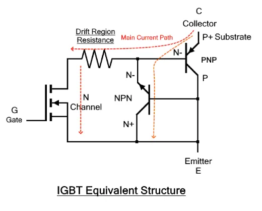
There are two types of Insulated Gate Bipolar Transistors: non-punch through IGBT (NPT IGBTs) and punch through IGBT (PT IGBTs). These two types are distinguished as follows: when the IGBT is designed with an N+ buffer layer, it is referred to as a PT IGBT; conversely, when the IGBT is designed without an N+ buffer layer, it is called an NPT IGBT. The presence of the buffer layer enhances the IGBT's performance. The operation of an IGBT is faster than that of a power BJT or power MOSFET.
Advantages and disadvantages of IGBTs
As expected, Insulated Gate Bipolar Transistors (IGBTs) present several pros and cons in comparison to other semiconductor devices such as bipolar transistors or power MOSFETs. These factors must be carefully weighed when considering their use in electronic designs.
IGBT advantages:
1. High voltage and current capabilities compared to bipolar transistors or power MOSFETs.
2. Typically do not latch like thyristors.
3. Can switch high current levels using low control voltage.
4. Very low on-resistance, ideal for many power switching applications.
5. Possess very high input impedance.
6. Voltage-controlled (like MOSFETs), requiring minimal current to switch high current levels.
7. Gate drive signals are easy to implement and do not require complicated circuitry: a simple positive voltage to turn the IGBT on and zero to turn it off.
8. High current density, resulting in smaller silicon chip sizes and, consequently, smaller package sizes for a given current level.
9. Higher power gain compared to both bipolar transistors and MOSFETs.
10. Faster switching speed compared to bipolar transistors.
11. Exhibit a lower ratio of gate-collector capacitance to gate-emitter capacitance than competing devices, resulting in improved Miller feedback effect performance and faster switching than bipolar transistors.
IGBT disadvantages
1. Unidirectional - cannot handle AC waveforms without supplementary circuitry.
2. Has a lower switching speed compared to a MOSFET.
3. Unable to block high reverse voltage.
4. May experience latching problems due to the PNPN structure resembling a thyristor within the device, although appropriate doping levels should suppress thyristor action.
5. More expensive than a bipolar transistor or a power MOSFET.
These are some of the more apparent pros and cons of employing an IGBT, but there may also be other factors to consider when evaluating its suitability for a specific electronic design.
Due to their advantages, IGBTs are widely utilized in numerous medium power switching applications. While they can function with AC, they require supplementary circuitry to facilitate bidirectional operation.
For bidirectional operation, IGBTs usually necessitate two devices of opposite polarity to accommodate both halves of the cycle. Such circuits are well-suited for power switching and various other power applications.
IGBT applications
The Insulated Gate Bipolar Transistor (IGBT) is employed in numerous power applications.
These semiconductor devices are highly beneficial for many electronic circuit designs because they bridge the gap between bipolar transistor technology and power FETs. As a result, they are used in a wide range of power applications:
- Various types of motor and traction control
- Switch-mode power supplies
- DC-AC inverters
- Pulse width modulation in various contexts
- AC and DC motor drives
- Driving various types of inductive loads
Circuit Diagram of an IGBT
Based on the fundamental construction of the Insulated Gate Bipolar Transistor, a basic IGBT driver circuit can be designed using PNP and NPN transistors, JFET, and MOSFET, as illustrated in the figure below. The JFET transistor is utilized to connect the collector of the NPN transistor to the base of the PNP transistor. These transistors represent the parasitic thyristor to form a negative feedback loop.
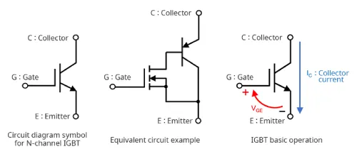
The RB resistor is connected to the BE terminals of the NPN transistor to ensure the thyristor does not latch up, which would cause the IGBT to latch up. The transistor depicts the current structure between any two adjacent IGBT cells. It allows the MOSFET to support most of the voltage. The circuit symbol of the IGBT, which includes three terminals—emitter, gate, and collector—is shown below.
IGBT Characteristics
The Insulated Gate Bipolar Transistor is a voltage-controlled device, requiring only a small voltage on the gate terminal to maintain conduction through the device.
Since the IGBT is voltage-controlled, it needs only a minimal voltage on the gate to sustain conduction, unlike BJTs, which require a continuous and sufficient base current to remain in saturation.
The IGBT can switch current in one direction, specifically in the forward direction (collector to emitter), whereas MOSFETs can switch current bidirectionally. This is because the IGBT is controlled only in the forward direction.
The operation of gate drive circuits for the IGBT is similar to that of an N-channel power MOSFET. The key difference lies in the IGBT's low resistance in the conducting channel when current flows through the device in its active state. Consequently, the current ratings for the IGBT are higher compared to a corresponding power MOSFET.
In conclusion
This overview covers the working and characteristics of the Insulated Gate Bipolar Transistor. We have seen that it is a semiconductor switching device with control capabilities akin to a MOSFET and output characteristics similar to a BJT. We hope this explanation has enhanced your understanding of the IGBT concept. For any further questions about the applications and advantages of an IGBT, please share your suggestions in the comment section below. Here is a question for you: What are the differences between BJT, IGBT, and MOSFET?
Related Articles
Thyristor vs Transistor: What are the Differences?
NPN Transistor? Construction, Working & Applications
PNP Transistor? Construction, Working & Applications


