


What Op-Amp IC is and How It works
IC 741
The IC 741 is the most widely used Op-Amp IC. This voltage amplifier inverts the input voltage at the output and is a common component in many electronic circuits.
Pin Configuration:
Let's examine the pin configuration and testing of 741 op-amps. Typically, the pins are numbered counterclockwise around the chip. This IC has 8 pins and offers excellent performance in integrator, summing amplifier, and general feedback applications. As a high-gain op-amp, the voltage on the inverting input can be kept nearly equal to Vin.
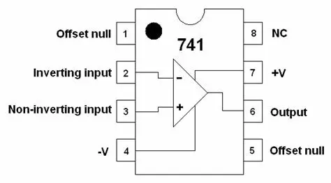
- Pin Configuration for Op-Amp IC 741
- Pin 1: Offset null.
- Pin 2: Inverting input terminal.
- Pin 3: Non-inverting input terminal.
- Pin 4: –VCC (negative voltage supply).
- Pin 5: Offset null.
- Pin 6: Output voltage.
- Pin 7: +VCC (positive voltage supply).
- Pin 8: No connection.
The primary pins in the 741 op-amp are pin 2, pin 3, and pin 6. In an inverting amplifier configuration, applying a positive voltage to pin 2 results in a negative output voltage through pin 6, indicating that the polarity has been inverted. In a non-inverting amplifier configuration, applying a positive voltage to pin 3 results in a positive output voltage through pin 6, maintaining the same polarity. The supply voltage (Vcc) typically ranges from 12 to 15 volts. When dual supplies (+Vcc/-Vcc) are used, they are generally equal in magnitude but opposite in polarity. It is crucial to remember that the operational amplifier is a high-gain, differential voltage amplifier. For a 741 operational amplifier, the gain is at least 100,000 and can exceed one million (1,000,000). This is a critical fact to keep in mind when incorporating the 741 into a circuit.
Applications of Op-Amp IC 741
There are many common application circuits using the IC741 op-amp, including adder, comparator, subtractor, integrator, differentiator, and voltage follower.
Below are some examples of circuits based on the 741 IC. In these examples, the 741 is used as a comparator rather than an amplifier. The distinction between the two is subtle but important. Even when used as a comparator, the 741 can detect weak signals for easier recognition. A comparator is a circuit that compares two input voltages: one is the reference voltage, and the other is the input voltage. This circuit compares a signal voltage applied at one input of an op-amp with a known reference voltage at the other input. The 741 op-amp has ideal transfer characteristics (output ±Vsat), and the output changes with an increment in the input voltage of 2mV.
LM324
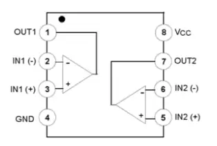
The LM324 is a quad op-amp integrated circuit known for its high stability and bandwidth, designed to operate from a single power supply over a wide voltage range. It offers several distinct advantages over standard operational amplifier types in single supply applications. Housed in a 14-pin dual in-line package, the LM324 contains four internally compensated, two-stage operational amplifiers, as shown in the figure.
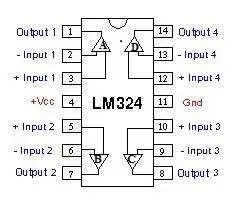
Pin Configuration for Op-Amp IC LM324
- Pin 1, 7, 8, and 14: Outputs of comparator
- Pin 2, 6, 9, and 13: Inverting inputs of comparator
- Pin 3, 5, 10, and 12: Non-inverting inputs of comparator
- Pin 11: Ground (0V)
- Pin 4: Supply voltage (5V)
Features:
- Internally frequency compensated for unity gain
- Large DC voltage gain of 100 dB
- Wide bandwidth of 1 MHz
- Wide power supply range: Single supply from 3V to 32V
- Essentially independent of supply voltage
- Differential input voltage range equal to the power supply voltage
- Large output voltage swing from 0V to V+ − 1.5V
Potential dividers of the LM324 are connected to the inverting and non-inverting inputs of the op-amp to provide some voltage at these terminals. The supply voltage is connected to +V, and –V is connected to ground. The output of this comparator will be logic high if the non-inverting terminal input is greater than the inverting terminal input. Conversely, when the inverting input is greater than the non-inverting input, the output will be logic low (0).
Working of Op-Amp IC LM324
When the power is applied to the non-inverting terminal and it is less than the inverting voltage of the op-amp, the output becomes zero, indicating no current flow. This follows the rule: when “+ > – = 1”, where the ‘+’ sign indicates the non-inverting terminal and the ‘-’ sign indicates the inverting terminal.
If the non-inverting voltage is greater than the inverting voltage, the output will be high.
In the LM324, the output is internally connected to some resistances and has a specific arrangement inside the IC, which differentiates it from other comparators. It is internally pulled-up, eliminating the need for an external resistor connection from the supply.
LM339
The LM339 is a widely used comparator designed for level detection, low-level sensing, and memory applications in automotive and industrial electronics. It features four built-in comparators that compare two input voltage levels and provide a digital output indicating the larger one.
These comparators have a unique characteristic: the input common-mode voltage range includes ground, even when operated from a single power supply voltage.
Pin Configuration:
- Pin 1, 2, 13, and 14:** Outputs of comparator
- Pin 3: Supply voltage (5V)
- Pin 4, 6, 8, and 10:** Inverting inputs of comparator
- Pin 5, 7, 9, and 11:** Non-inverting inputs of comparator
- Pin 12: Ground (0V)
Features:
- Signal or dual supply operation
- Wide operating supply range (VCC = 2V to 36V)
- Maximum rating: 2V to 36V
- Tested to 30V: Non-V Devices
- Input common-mode voltage includes ground
- Low supply current drain (IF = 0.8mA)
- Open collector outputs for wired connection
- Low input bias current (25nA)
- Low output saturation voltage
- Output compatible with TTL, DTL, and CMOS logic systems
- Differential input voltage range equal to the power supply voltage
Potential dividers of the LM339 are connected to the inverting and non-inverting inputs of the op-amp to provide some voltage at these terminals. The supply voltage is connected to +V, and –V is connected to ground. The output of this comparator will be logic high if the non-inverting terminal input is greater than the inverting terminal input.
Working of Op-Amp IC LM339
When the power is applied to the non-inverting terminal and it is less than the inverting voltage of the op-amp, the output becomes zero, meaning there is no current flow. This follows the principle: when “+ > – = 1”, where the ‘+’ sign represents the non-inverting terminal and the ‘-’ sign represents the inverting terminal.
If the non-inverting voltage is greater than the inverting voltage, current will flow through the device.
The LM339 acts as an open-collector, which is why a resistor is connected from the supply. If the resistor is removed, there will be no current flow in the circuit.
LM358
The LM358 op-amps are used in transducer amplifiers, DC gain blocks, and conventional op-amp circuits, which can now be more easily implemented in single power supply systems. For example, the LM358 op-amp can be directly operated off the standard +5V power supply voltage used in digital systems, providing the required interface electronics without needing the extra ±15V power supplies.
It comes in an 8-pin DIP package as shown below.
Pin Description:
- Pin 1 and 7: Outputs of comparator
- Pin 2 and 6: Inverting inputs
- Pin 3 and 5: Non-inverting inputs
- Pin 4:Ground (GND)
- Pin 8: VCC+
Features:
- Internally frequency compensated for unity gain
- Large DC voltage gain: 100 dB
- Wide bandwidth
- Wide power supply range: single supply from 3V to 32V
- Very low supply current drain, essentially independent of supply voltage
- Low input offset voltage: 2 mV
- Input common-mode voltage range includes ground
- Differential input voltage range equal to the power supply voltage
- Power drain suitable for battery operation
Advantages:
- Two internally compensated op amps
- Eliminates the need for dual supplies
- Allows direct sensing near GND and VOUT also goes to GND
- Compatible with all forms of logic
- Power drain suitable for battery operation
Working of LM358:
The inverting input of the comparator LM358 (pin 2) is given a fixed voltage in the ratio 47k:10k, and the non-inverting input of the comparator is pulled down and connected to the sensing terminal. When the resistance between the positive supply and the non-inverting input is high, the non-inverting input is less than the inverting input, making the comparator output logic low at pin 1. When the resistance decreases, making the voltage available to the non-inverting input higher than the inverting input, the output of the comparator becomes logic high.
CA 3130 Op Amp
The CA3130 is an excellent op-amp with very low input current requirements. In its off mode, the output is in the zero state. It operates at 15MHz and is a BiMOS IC with MOSFET inputs and a bipolar output. MOSFET transistors at the inputs provide very high input impedance, with input currents as low as 10pA. This IC demonstrates high-speed performance, combining the advantages of both CMOS and bipolar transistors. PMOS transistors at the inputs allow for a common-mode input voltage capacity down to 0.5 volts below the negative rail, making it ideal for single supply applications.
The output features a CMOS transistor pair that swings the output voltage within 10mV of either supply voltage terminal. The CA3130 operates from 5 to 16 volts and can be phase compensated with a single external capacitor. It also includes terminals for adjusting offset voltage and strobing.
CA 3140 Op Amp
The CA3140 is a 4.5MHz BiMOS op-amp with MOSFET inputs and a bipolar output. It incorporates PMOS transistors and high-voltage bipolar transistors internally. Its inputs are protected by gate-protected MOSFETs (PMOS), providing very high input impedance typically around 1.5 teraohms. Input current requirements are very low, around 10pA. The CA3140 exhibits rapid response and high-speed performance.
The output is protected against damage from load terminal shorting. Its input stage includes PMOS FETs, enhancing its common-mode input voltage capability to as low as 0.5 volts. The IC is internally phase compensated for stable operation and includes terminals for additional frequency roll-off and offset nulling.
TL071 Op Amp
The TL071 is a low-noise op-amp with JFET inputs. It operates with wide common-mode range and consumes minimal current. It exhibits very low input bias and offset currents. The output is short-circuit protected and features a high slew rate of 13 V/μs, ensuring latch-free operation. The TL071 is particularly suitable for high-fidelity audio preamplifier circuits. Both the TL071 and TL072 contain a single op-amp, while the TL074 is a quad op-amp with four operational amplifiers inside.
TL082 Op Amp
The TL082 is a dual op-amp with separate inputs and outputs. It features JFET inputs and bipolar outputs. The IC offers a high slew rate, low input bias, low offset current, and low offset voltage. Its inputs can be biased with very low input currents, and its output is protected against short circuits. The TL082 operates latch-free and includes internal frequency compensation.
LM311 Op Amp
The LM311 is a single op-amp capable of driving DTL, RTL, TTL, or MOS circuits. Its output can switch up to 50 volts and 50mA current. Operating across a wide range of supply voltages from 5V to 30V, it requires only a single supply. The LM311 can directly drive relays, solenoids, etc., if the current requirement is less than 50mA.
The pin configuration of the LM311 differs from other op-amps: pin 3 is the inverting input, and pin 2 is the non-inverting input. It has two outputs: pin 7 (positive output) sinks current, while pin 1 (negative output) serves as the emitter of the output transistor. Normally, the output transistor is in the off state, with its collector pulled to Vcc. When its base receives more than 0.7 volts, it saturates and turns on, sinking current to turn on the load. Unlike other op-amps, the LM311 sinks current, causing the output to go low when triggered.
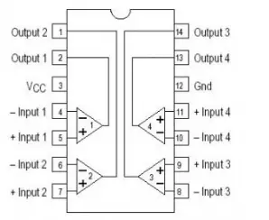
IC 747
The IC 747 is a dual operational amplifier designed for general-purpose use, incorporating two 741 op-amps within its structure. Each op-amp shares a common bias network and power supply leads but operates independently in all other aspects. The IC is packaged in a 14-pin dual in-line package (DIP).
- Pin Configuration:
- Pin 1: Inverting input terminal of op-amp 1
- Pin 2: Non-inverting input terminal of op-amp 1
- Pin 3: Offset null terminal of op-amp 1
- Pin 4: Negative supply voltage (-V)
- Pin 5: Offset null terminal of op-amp 2
- Pin 6: Non-inverting input terminal of op-amp 2
- Pin 7: Inverting input terminal of op-amp 2
- Pin 8: Offset null terminal of op-amp 2
- Pin 9: Positive supply voltage (+V) of op-amp 2
- Pin 10: Output of op-amp 2
- Pin 11: No connection (NC)
- Pin 13: Positive supply voltage of op-amp 1
- Pin 14: Offset null terminal of op-amp 1
Features of 747 op-amp
- Dual supply voltage: ±1.5V to ±15V
- No frequency compensation required
- Short-circuit protection
- Wide common-mode and differential voltage ranges
- Low power consumption
- Unity gain stable
- No latch-up
- Balanced offset null
- Supply current is less than 300 μA per amplifier at 5V
How to Test an Op-Amp IC?
Operational amplifiers (Op-Amps) are integral components in electronic circuits, serving as amplifiers, comparators, voltage followers, summing amplifiers, and more. Common Op-Amps like the 741, TL071, CA3130, and CA3140 share similar pin configurations, making a universal tester essential for troubleshooting and servicing. This tool is straightforward to construct and indispensable on the workbench of hobbyists and technicians.
The tester is built around an 8-pin IC base where the Op-Amp to be tested is inserted. Pin 2 (inverting input of the IC) is connected to a potential divider (R2, R3) that provides half of the supply voltage to pin 2. Pin 3 (non-inverting input) of the IC base connects to VCC through R1 and a push-to-on switch. Pin 6, the output, connects to a visual indicator LED via a current-limiting resistor (R4).
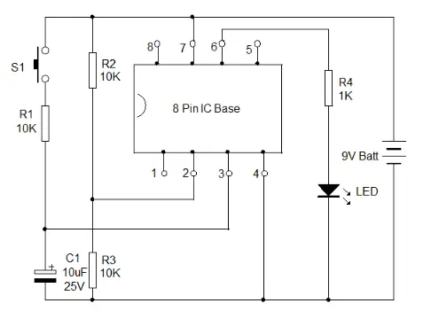
Voltage Comparator Design
The circuit is configured as a voltage comparator. Insert the IC into the socket ensuring correct orientation, where the notch on the left side of the IC aligns with the notch in the IC base. In comparator mode, the output of IC1 goes high when its pin 3 receives a higher voltage than pin 2. For instance, if pin 2 receives 4.5 volts (assuming a 9V battery), and pin 3 receives 0 volts, the output remains low, and the LED remains unlit.
Pressing S1 causes pin 3 to receive a higher voltage than pin 2, causing the output of IC1 to go high and light up the LED. This illumination indicates proper functioning of the internal circuitry of the IC.
Testing Topologies
There are three testing topologies for op-amps:
- 1. The two operational amplifier test loop
- 2. Self-test loop
- 3. Three op-amp loop


