


LTC2055 Amplifier:Description,Features & Applications
What is the LTC2055 Amplifier?
The exceptionally low offset voltage and low noise of Analog Devices' (formerly known as Linear Technology) LTC2055 precision optical amplifier are well-known. It is hence perfect for highly precise applications.
Description of the LTC2055 Amplifier
A micropower optical amplifier is the LTC2055. Minimal Sound and Helicopter Balance To guarantee minimal input offset voltage, it makes use of zero-drift technology. Temperature- and time-related drift and drag are almost completely removed. There is a broad range of supply voltages that the gadget can run on. It features swing inputs and outputs from rail to rail. Because of this, it may be used with a wide range of designs. Battery-powered systems are a good fit for the LTC2055 because of its low quiescent current.
Key Specifications of the LTC2055 Amplifier
|
Parameter |
Specification |
|
Supply Voltage |
2.7V to 12.6V (±1.35V to ±6.3V) |
|
Input Offset Voltage |
3µV (typical) |
|
Input Offset Voltage Drift |
0.015µV/°C (typical) |
|
Input Bias Current |
5pA (typical) |
|
Input Voltage Noise |
220nVpp (0.1Hz to 10Hz, typical) |
|
Gain Bandwidth Product |
3.5MHz |
|
Slew Rate |
0.3V/µs |
|
Supply Current |
1.2mA (per amplifier, typical) |
|
Output Voltage Swing |
Rail-to-Rail |
|
Common Mode Rejection Ratio (CMRR) |
150dB (typical) |
|
Power Supply Rejection Ratio (PSRR) |
140dB (typical) |
|
Operating Temperature Range |
-40°C to 125°C |
|
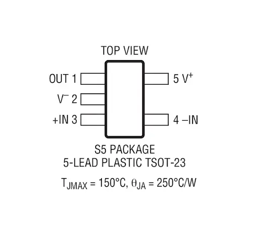
Package Options |
MS8, DFN (3mm x 3mm) |
Key Features of the LTC2055 Amplifier
- Low Offset Voltage
- Low Noise
- Zero-Drift
- Low Power Consumption
- Rail-to-Rail Input and Output
- Wide Supply Voltage Range
Working Principle of the LTC2055 Amplifier
A zero-drift optical amplifier with great sensitivity and stability, the LTC2055 is intended for low-frequency applications. Through the use of a process known as auto-drift, the amplifier gradually lowers offset pressure and slip.
Key Components and Concepts:
1. Auto-Zeroing Technique:
- The LTC2055 uses a technique where the input offset voltage is periodically sampled and corrected. This involves alternating between two phases:
- Sampling Phase: During this phase, the amplifier samples the offset voltage and stores it on a capacitor.
- Correction Phase: In this phase, the stored offset voltage is subtracted from the input signal, effectively canceling the offset.
2. Input Stage:
- The LTC2055 is engineered to have low bias current and high common mode rejection in its input phase. For amplifier performance in delicate applications, this phase is essential.
3. Chopper Stabilization:
- The input signal is modulated (mixed) to a higher frequency, amplified, and then demodulated back to its original frequency in order to achieve stabilization with the LTC2055 chopper. Low frequency noise, such as 1/f noise, which is frequently present in conventional operational amplifiers, is eliminated by this approach.
4. Low Offset Voltage and Drift:
- The LTC2055 are perfect for precise measurements because of their automatic reset and cutoff stabilization mechanisms, which allow them to give very low input offset voltages, very low voltages (usually in the microvolt range), and very little drift over time and over a variety of temperatures.
5. High Common-Mode Rejection Ratio (CMRR):
- The LTC2055 has a high CMRR, which is essential in rejecting noise and interference from common-mode signals, further enhancing its precision in differential measurements.
Applications of the LTC2055 Amplifier
- High-Precision Data Acquisition Systems
- Precision Analog Signal Conditioning
- Instrumentation Amplifiers
- Medical Instrumentation
- Weighing Scales
- Low-Level Signal Processing
- Analog Filters
- Voltage References
- Data Acquisition Systems
- Analog Multipliers
- High-Precision Voltage Followers
- High-Resolution Analog-to-Digital Converters (ADCs)
- Bridge Amplification
- Signal Isolation
- Noise-Cancellation Systems
- Phase-Locked Loops (PLLs)
- High-Precision Measurement Systems
- Precision Voltage Regulators
- High-Resolution DACs
- Scientific Research Equipment
- Low-Level Signal Detection
- Calibration Systems
LTC2055 Amplifier vs. AD8628 vs. OP07 vs. OPA2188 vs. MAX40008
|
Feature |
LTC2055 |
AD8628 |
OP07 |
OPA2188 |
MAX40008 |
|
Type |
Precision Op-Amp |
Precision Op-Amp |
Precision Op-Amp |
Precision Op-Amp |
High-Speed Op-Amp |
|
Supply Voltage |
±2.5V to ±18V |
±2.5V to ±18V |
±3V to ±15V |
±2.5V to ±18V |
±1.5V to ±5.5V |
|
Input Offset Voltage |
25 µV (max) |
25 µV (max) |
50 µV (max) |
25 µV (max) |
25 µV (max) |
|
Input Bias Current |
2 pA (typ) |
10 pA (typ) |
1 nA (typ) |
0.5 pA (typ) |
0.3 pA (typ) |
|
Gain Bandwidth Product |
500 kHz (typ) |
10 MHz (typ) |
1 MHz (typ) |
10 MHz (typ) |
7 MHz (typ) |
|
Slew Rate |
0.2 V/µs (typ) |
0.5 V/µs (typ) |
0.5 V/µs (typ) |
1 V/µs (typ) |
4 V/µs (typ) |
|
Total Harmonic Distortion (THD) |
0.01% (typ) |
0.0005% (typ) |
0.01% (typ) |
0.0001% (typ) |
0.001% (typ) |
|
CMRR |
130 dB (typ) |
120 dB (typ) |
110 dB (typ) |
120 dB (typ) |
120 dB (typ) |
|
PSRR |
130 dB (typ) |
120 dB (typ) |
110 dB (typ) |
120 dB (typ) |
120 dB (typ) |
|
Noise Density |
5 nV/√Hz (typ) |
7 nV/√Hz (typ) |
15 nV/√Hz (typ) |
7 nV/√Hz (typ) |
6.5 nV/√Hz (typ) |
|
Package Options |
8-SOIC, 8-SOIC (LFCSP) |
8-SOIC, 8-DIP |
8-DIP, 8-SOIC |
8-SOIC, 8-DIP |
8-SOIC |
.webp)
.webp)
Notes:
- LTC2055: Is well-known for having low noise and an extremely low offset voltage, which makes it perfect for precision applications where these characteristics are crucial.
- AD8628: Suitable for high precision signal processing, it has a smaller THD and a larger gain bandwidth than other precision op amps.
- OP07: A classic precision op-amp, widely used and known for its stability and low offset voltage, though its bandwidth is lower compared to more modern options.
- OPA2188: Provides a better conversion rate ratio, excellent precision, low noise and distortion voltage, and is optimized for speedier applications.
- MAX40008: Fast operational amplifier with good bandwidth and conversion rate performance. It does, however, run at a lower voltage than other precision operational amplifiers.
Advantages of the LTC2055 Amplifier
- Ultra-Low Offset Voltage
- Low Offset Voltage Drift
- Low Noise
- Low Input Bias Current
- Wide Supply Voltage Range
- Rail-to-Rail Output
- High Open-Loop Gain
- High Slew Rate
- Low Total Harmonic Distortion (THD)
- Low Quiescent Current
- Excellent CMRR (Common-Mode Rejection Ratio)
- High PSRR (Power Supply Rejection Ratio)
- Low Total Input Noise
- Stable Over Temperature
- High Gain-Bandwidth Product
What are the key features of the LTC2055 amplifier?
- Zero-drift operation with low offset voltage (2 µV maximum).
- Low input bias current (less than 30 pA).
- Wide supply voltage range from 2.7V to 12V.
- Rail-to-rail output.
- Low noise (0.5 µV peak-to-peak in 0.1Hz to 10Hz bandwidth).
- Low power consumption (350 µA typical supply current).
- Available in dual-channel (LTC2055) and single-channel (LTC2054) versions.
What applications are suitable for the LTC2055?
- Precision data acquisition systems.
- Medical instrumentation.
- Strain gauge amplifiers.
- Thermocouple amplifiers.
- Portable instrumentation.
- Sensor signal conditioning.
- Low-frequency noise-sensitive applications.
What is zero-drift in the context of the LTC2055?
- The input offset voltage is continually corrected by the zero-drift amplifier. Even under challenging conditions, the LTC2055 is incredibly stable and accurate because it keeps its offset value exceptionally low throughout the whole time and temperature range.
How does the LTC2055 achieve low noise performance?
- By removing offset and 1/f noise through the use of a novel auto-calibration technique, the LTC2055 offers low noise performance over a broad frequency range.
What is the power supply requirement for the LTC2055?
- With a voltage range of 2.7V to 12V, the LTC2055 can function in a variety of power-related scenarios, including those involving battery-powered devices.
How does the rail-to-rail output benefit applications?
- The LTC2055 can oscillate extremely close to the power rails thanks to its rail-to-rail output, which maximizes its dynamic range and makes it usable in low voltage applications where every millivolt of signal range matters.
What is the maximum offset voltage drift of the LTC2055?
- The smallest temperature variation at out-of-phase voltages is ensured by the LTC2055's 0.015 µV/°C out-of-phase voltage.
Is the LTC2055 suitable for use in high-impedance sensor applications?
- Yes, the LTC2055 is appropriate for high impedance sensor applications where the lowest possible sensor load is crucial because of its low input bias current (less than 30 pA).
Related Articles
Voltage Amplifier vs Power Amplifier: What’s the Differences?
Push-pull Amplifier :Overview and Working Principle
What is TL074 Operational Amplifier?


