


Why Using Op Amps as Comparators?
INTRODUCTION
A comparator, much like an operational amplifier (op amp), features two input terminals - inverting and noninverting - and an output that typically swings from rail to rail. Similarly, an op amp shares characteristics such as low offset, high gain, and high common-mode rejection.
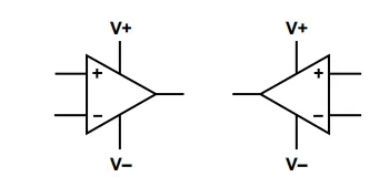
The primary distinction lies in their outputs: a comparator produces a logic output indicating the higher potential input, often tailored to be TTL or CMOS compatible, remaining at one rail or transitioning rapidly between the two. On the other hand, an op amp furnishes an analog output, not necessarily close to the supply rails, positioned somewhere in between. Although designed for closed-loop applications with feedback, modern op amps can approach their supply rails.
The question arises: Why not employ op amps as comparators? Op amps offer advantages like high gain, low offset, and high common-mode rejection, often at a lower cost than comparators. Moreover, they are commonly available in packages of two or four, providing practicality in certain scenarios.
However, cautionary advice emerges against using op amps as comparators. While comparators excel in open-loop systems, logic circuit driving, and high-speed operation even under overdrive conditions, op amps are not designed for these purposes. Op amps function best in closed-loop configurations, driving simple resistive or reactive loads, and should avoid being overdriven into saturation.
Despite the tempting aspects, the remainder of this document underscores the reasons behind considering op amps as comparators and highlights potential unforeseen consequences, ultimately advising against such usage.
WHY OPT FOR AN OP AMP AS A COMPARATOR?
- Convenience
- Economy
- Low Input Bias Current (IB)
- Low Voltage Offset (VOS)
There are multiple reasons for opting to use operational amplifiers (op amps) as comparators, ranging from technical considerations to economic factors. Op amps are not only manufactured as individual devices but also in duals and quads, featuring two or four op amps on a single chip. These multi-op amp configurations are more cost-effective than purchasing separate op amps, and they occupy less board space, providing additional cost savings. While it may be economical to utilize the spare op amp in a quad as a comparator, it is crucial to note that this practice is not considered good design.
Comparators, designed for clean and swift switching, sometimes exhibit inferior DC parameters compared to many op amps. Consequently, using an op amp as a comparator might be convenient in applications requiring attributes like low Voltage Offset (VOS), low Input Bias (IB), and wide Common-Mode Range (CMR). However, this approach is not recommended if high speed is a critical requirement.
WHY AVOID USING AN OP AMP AS A COMPARATOR?
- Speed
- Inconvenient Input Structures
- Inconvenient Logic Structures
- Stability/Hysteresis
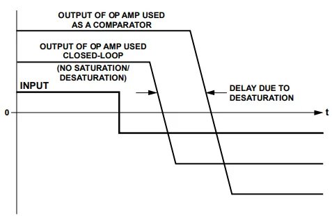
Numerous reasons discourage the use of op amps as comparators, primarily speed-related concerns. Additionally, considerations regarding output levels, stability (including hysteresis), and various input structure aspects contribute to this avoidance. Although most comparators exhibit high speed, as do some op amps, the expectation of low speed when using an op amp as a comparator arises from the inherent design differences. Comparators are designed for large differential input voltages, while op amps typically operate in closed-loop configurations with minimized input voltages due to negative feedback. Overdriving an op amp, even by a few millivolts, may lead to saturation in some of its stages, resulting in a slower response compared to unsaturated operation.
The recovery time of an op amp after overdrive is likely to exceed its typical group delay (the time a signal takes from input to output) and often correlates with the degree of overdrive. Due to limited characterization of op amps for recovery times at varying overdrive levels, users must experimentally determine the delays expected in a specific application. The value used in design calculations should be at least twice the worst delay observed in tests to account for potential variations among samples.
A purpose-built comparator's output is tailored to drive specific logic families, often featuring a separate supply for the output stage to ensure correct logic levels. In contrast, modern op amps typically offer rail-to-rail output, meaning their maximum positive level is close to the positive supply, and the minimum negative level is close to the negative supply. When an op amp and logic share the same supply, a rail-to-rail op amp can successfully drive CMOS and TTL logic families. However, if the op amp and logic have different supplies, additional interface circuitry is necessary.
The simplest interface circuits are inverters, which can be constructed using NPN transistors or, more conveniently, N-channel MOSFET transistors. RB sets the transistor base current, while RL sets the collector/drain current. Lower values result in faster inverters but consume more power. The N-channel MOS device should have a low gate threshold voltage (<2 V) and a gate-source breakdown voltage greater than the maximum output voltages of the op amp, typically ±25 V.
Even when the op amp and logic use different supplies, their relationships are crucial. The op amp's positive supply, +VA, must be more positive than the logic's negative supply, −VL, by at least 3 V to activate the transistor or MOSFET gate. Additionally, the op amp's negative supply must not be positive relative to the logic's negative supply, although they may be connected. Adherence to the absolute maximum ratings of all devices used is essential.
A complementary MOS inverter can be constructed using a P-channel and an N-channel MOSFET, offering the advantage of drawing no standby current. However, it does exhibit a large current spike during switching when both devices are briefly turned on simultaneously. In this configuration, the op amp's positive supply, +VA, must be equal to or greater than the logic's positive supply, +VL. Similarly, the op amp's negative supply must be equal to or less than the logic's negative supply.
An alternative method to ensure correct logic interface levels involves using a clamp amplifier like the AD8036. A clamp amplifier features positive and negative reference terminals, clamping its output within 30 mV of the reference voltages if it attempts to go above or below the positive and negative limits. Connecting the positive and negative logic supplies to the reference inputs allows the amplifier output to safely drive the logic, even if the amplifier supplies are outside the logic supplies.
When op amps are used as comparators, they tend to respond more slowly than expected due to saturation. While there are likely few applications where op amps used as comparators are required to drive emitter-coupled logic (ECL), Figure 7 illustrates an interface using three resistors, R1, R2, and R3. These resistors are selected to ensure that when the op amp output is at its positive limit, the level at the ECL gate input is −0.8 V, and when it is at its negative limit, the voltage is −1.6 V. The ratio of R1, R2, and R3 is set accordingly, considering the compromise between speed and power economy.
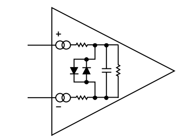
Several considerations arise regarding the inputs of op amps used as comparators. The assumption of infinite input impedance, while reasonable for voltage-feedback op amps, is invalid for current-feedback (transimpedance) op amps with very low impedance at their inverting inputs. Therefore, they should not be used as comparators. Actual characteristics of input impedance and bias currents must be taken into account, and calculations should be made to ensure the design works with the expected values. Some op amps feature input stages like long-tailed pairs of transistors or FETs, providing high input impedance even with large differential voltages. However, more complex input structures, such as bias-compensated or rail-to-rail input stages, may not respond well to large differential input voltages. Protection circuitry, as shown in Figure 9, illustrates one of many structures addressing this issue. The device has high input impedance for differential inputs below ±0.6 V, but the protection diodes conduct and the differential input impedance drops abruptly above that range. In applications where the differential input is limited to a few tens or hundreds of millivolts, these effects become crucial.


