


Diode:Construction,Types & Working
What is a Diode?
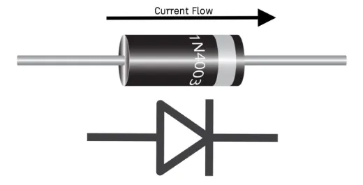
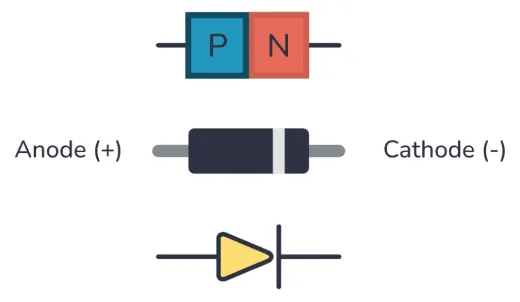
The term "di" signifies "two," while "ode" refers to "electrodes," indicating a device or component with two electrodes: the Anode "+" (P) and Cathode "-" (N).
A diode serves as a two-terminal, unidirectional power electronics device. It stands as the foundational invention in the realm of semiconductor electronics devices, with numerous diode variants subsequently developed. Nevertheless, the semiconductor diode remains the most commonly utilized type.
Typically, silicon serves as the primary material for diode fabrication. However, alternative semiconductor materials like germanium or germanium arsenide are also employed.
A diode permits current flow solely in one direction while impeding current flow in the opposite direction. It exhibits low resistance (ideally zero) in one direction and high resistance (ideally infinite) in the other direction.
Construction of Diode
There are two types of semiconductor materials: intrinsic and extrinsic semiconductors. An intrinsic semiconductor is a pure semiconductor where holes and electrons are present in equal amounts at room temperature. In an extrinsic semiconductor, impurities are added to increase the number of holes or electrons. These impurities are either trivalent (such as boron, indium, aluminum) or pentavalent (such as phosphorous, arsenic, antimony).
A semiconductor diode consists of two layers. One layer is made from a P-type semiconductor, and the other is made from an N-type semiconductor.
When trivalent impurities are added to silicon or germanium, an increased number of holes result, leading to a positive charge. This layer is thus called the P-type layer.
When pentavalent impurities are added to silicon or germanium, an increased number of electrons result, leading to a negative charge. This layer is thus called the N-type layer.
A diode is created by joining the N-type and P-type semiconductors together. This combination forms a device known as a PN Junction Diode, named for the P-type and N-type semiconductor materials used.
A junction forms where the P-type and N-type layers meet, referred to as the PN junction.
A diode has two terminals: one from the P-type layer, known as the Anode, and the other from the N-type material, known as the Cathode. The following figure illustrates the basic construction of the diode.
Working of Diode
In the N-type region, electrons are the majority charge carriers while holes are the minority carriers. In the P-type region, holes are the majority charge carriers and electrons are the minority carriers. Due to the concentration difference, majority charge carriers diffuse and recombine with opposite charges, forming positive or negative ions. These ions accumulate at the junction, creating what is known as the depletion region.
When the anode terminal of the diode is connected to the negative terminal and the cathode to the positive terminal of a battery, the diode is said to be in reverse bias.
Conversely, when the anode terminal is connected to the positive terminal and the cathode to the negative terminal of the battery, the diode is said to be in forward bias.
Operation of Diode in Reverse Bias Condition
When the diode is in reverse bias, free electrons diffuse into the P-type region and recombine with holes, creating negative ions. Similarly, holes diffuse into the N-type region and recombine with electrons, creating positive ions.
When such voltage is applied to the circuit, immobile ions establish a depletion region as depicted in the preceding illustration. The breadth of this depletion region is considerable, thereby preventing the passage of additional holes or electrons across the junction.
Under such circumstances, even when supplied with the rated voltage, there is an absence of electron or hole flow. Consequently, the diode behaves akin to an open switch.
In this scenario, a nominal current does trickle through the circuit. Termed as reverse saturation current or reverse leakage current, this current arises from the presence of minority charge carriers. Nonetheless, its magnitude is insufficient to facilitate diode conduction.
Upon elevating the voltage to the reverse breakover level, minority charge carriers attain heightened kinetic energy, leading to collisions with atoms. This collision results in the rupture of covalent bonds and the generation of a significant number of electron-hole pairs, thereby fostering a substantial current flow.
Such a surge in current can potentially damage the diode; thus, as a standard practice, the diode is not typically connected in a reverse bias configuration.
Operation of Diode in Forward Bias Condition
When the anode is linked to the positive terminal of the battery and the cathode to the negative terminal, the anode assumes a positive polarity relative to the cathode, establishing a forward bias for the diode.
Subsequently, as we incrementally augment the supply voltage, a minor increase fails to provide the majority charge carriers with adequate energy to traverse the depletion region.
Under forward bias conditions, the depletion region contracts significantly in width. Exceeding the forward breakover voltage threshold, which is 0.7V for silicon and 0.3V for germanium, furnishes the majority charge carriers with ample energy to surmount the depletion region.
Upon surpassing this voltage threshold, the majority charge carriers commence flowing through the circuit, rendering the diode conductive.
Throughout this operational mode, there is a minute voltage drop, known as the on-state voltage drop. The schematic representation of this mode is illustrated in the accompanying figure.
VI-Characteristics of Diode
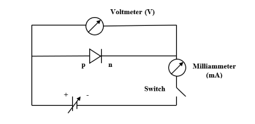
The voltage-current (VI) characteristic of the diode delineates the correlation between diode current and voltage. Represented graphically, it plots voltage on the X-axis and current on the Y-axis.
The schematic arrangement employed to derive the VI characteristic of the diode is depicted in the illustration below.
This characteristic manifests in two distinct segments:
1. Forward Bias
2. Reverse Bias
In the absence of applied voltage, the circuit sustains zero current flow. This state is denoted by point ‘O,’ signifying a condition where both voltage and current register at zero.
Forward Bias
When the P-type material or anode is connected to the positive terminal of the battery and the N-type material or cathode is connected to the negative terminal, the diode is in forward bias.
A variable resistor regulates the applied voltage, which is gradually increased. Current will not flow until the voltage surpasses the forward breakover voltage, as the initial voltage is insufficient to move charge carriers across the layers.
For silicon, the breakover voltage is 0.7V, and for germanium, it is 0.3V. Once the voltage exceeds this threshold, it becomes sufficient to move charge carriers from one layer to another, enabling current flow through the diode.
In the characteristics curve, segment OP is non-linear, representing the initial phase where the voltage is below the forward breakover voltage and the current is minimal.
Segment PQ illustrates the voltage exceeding the forward breakover voltage, where current increases linearly.
Under these conditions, the diode acts as a closed switch, permitting current flow. For an ideal diode, the on-state resistance is zero, and it functions as a perfect conductor.
Reverse Bias
In reverse bias, the N-type material or cathode is connected to the negative terminal of the battery. This configuration is known as a reverse bias connection.
In this setup, the voltage is gradually increased using a variable resistor, but this voltage remains insufficient to induce current flow.
This is because the junction between the P-type and N-type layers is in reverse bias, resulting in a substantial depletion width. Consequently, the applied voltage cannot mobilize the charge carriers.
Therefore, current does not flow through the diode. The corresponding curve in this mode is OA. As depicted in the graph, a very small current flows due to minority charge carriers, but this current is inadequate to activate the diode.
When the applied voltage exceeds the reverse breakdown voltage, a significant current flows due to avalanche breakdown. This is represented as segment AB in the graph.
Types of IGBTs
Light Emitting IGBT
Laser IGBT
Avalanche IGBT
Zener IGBT
Schottky IGBT
Photodiode IGBT
PN junction IGBT
Light Emitting IGBT (LED)
When a current flows between the electrodes in this IGBT, it emits light. In essence, light is generated when a sufficient forward current passes through it. In many IGBTs, this emitted light may not be visible due to certain frequency levels. LEDs come in various colors, including tricolor LEDs capable of emitting three colors simultaneously. The emitted light's color is determined by the semiconductor's energy gap.
Laser IGBT
This IGBT is distinct as it emits coherent light. It finds extensive use in CD drives, DVDs, and laser devices. While Laser IGBTs are more expensive than LEDs, they are cheaper compared to other laser sources. Their limited lifespan is their only drawback.
Avalanche IGBT
Belonging to the reverse bias type, this IGBT operates on the avalanche effect. When the voltage drop remains constant and independent of current, avalanche breakdown occurs. They exhibit high sensitivity levels, making them suitable for photodetection purposes.
Zener IGBT
This type of IGBT is highly useful as it can provide a stable reference voltage. Operating in reverse bias, it breaks down when a certain voltage threshold is reached. By limiting the current passing through the resistor, a stable voltage is produced. Zener IGBTs find wide application in power supplies for providing reference voltages.
Schottky IGBT
With a lower forward voltage compared to other silicon PN junction IGBTs, Schottky IGBTs exhibit a voltage drop typically ranging between 0.15 and 0.4 volts at low currents. They are constructed differently to achieve this performance and are extensively utilized in rectifier applications.
Photodiode
A photodiode can detect even minute current flows resulting from light exposure. These are particularly useful in light detection applications. Operating in reverse bias, photodiodes are employed in solar cells and photometers, and they can even be used to generate electricity.
PN Junction IGBT
Also known as rectifier IGBTs, PN junction IGBTs are utilized in the rectification process and are composed of semiconductor material. They consist of two layers of semiconductors—one doped with P-type material and the other with N-type material. The junction formed by the combination of these layers is termed the PN junction, hence the name PN junction IGBT.
PN junction IGBTs allow current to flow in the forward direction while blocking it in the reverse direction.
Related Post:
Insulated Gate Bipolar Transistor:Features and Pinout
Explanation of the Working Principle of Photodiodes
PNP Transistor? Construction, Working & Applications
Advantages of Diodes
PN junction diodes offer several advantages over vacuum diodes, including:
- Compact size
- Minimal space requirement
- Lightweight
- High reliability in operation
- Low power consumption
- Superior lifespan and efficiency
- Low internal resistance
- Easy installation and maintenance
- Simple and robust construction
- Cost-effective and readily available
Applications of Diodes
Diodes serve numerous functions in power electronics. As a unidirectional two-terminal device, a diode permits current flow in one direction while obstructing it in the opposite direction. This property makes diodes suitable for applications such as:
- Rectifiers
- Voltage multiplier circuits
- Over-voltage limiters
- Clipper and clamper circuits
- Reverse current protection circuits
- Digital logic gates
Additionally, diodes are utilized in solar panels to prevent reverse current flow and to bypass the solar plate. They also play a role in modulating and demodulating communication signals.
There are numerous other types of diodes designed for various specific applications, such as:
- The photodiode, which converts photon energy into electrical energy.
- The Light Emitting Diode (LED), used for illumination.
- The Zener diode, employed as a voltage regulator.
- The tunnel diode, utilized in RF circuits.
- The variable capacitance diode, used for tuning purposes.


